Packaging chip and packaging method thereof

a technology of packaging chip and chip body, applied in the field of packaging chip, can solve the problems of minute dust entering, damage to the chip body, signal loss through the wire, etc., and achieve the effect of reducing packaging time and cost and improving plating speed

Inactive Publication Date: 2006-12-07
SAMSUNG ELECTRONICS CO LTD +1
View PDF8 Cites 6 Cited by
  • Summary
  • Abstract
  • Description
  • Claims
  • Application Information

AI Technical Summary

Benefits of technology

[0009] An aspect of the present general inventive concept is to provide a packaging chip in which a viahole formed in a packaging wafer is plated with a seed layer stacked on an inner side of the viahole to prevent voids or cracks from occurring during the plating and to improve a plating speed so as to reduce packaging time and cost and a method of manufacturing the packaging chip.

Problems solved by technology

Electronic packaging chips used in various electronic products include micro electronic circuits and thus may be damaged by external impacts.
However, if the wires are used, minute dust may flow into the packaging chip through the viahole and signal loss may occur through the wires.
As a result, cracks or voids may slightly occur in the viahole.
If voids occur, impurities inside the voids rust, which may break down the packaging chip.
The impurities inside the voids may be heated by a current supplied from an external source and thus damaged.
If cracks occur, minute dust flows into an element from the outside, and thus the element may malfunction.
However, the seed layer is formed only at a low portion, and a plating speed becomes slow.
This increases cost.
As a result, the unit cost of a packaging chip is increased.
Also, cracks may occur, or the packaging chip may be damaged due to a low adhesive strength between a packaging wafer and the connecting electrode.
Thus, the manufacturing yield of packaging chips is decreased.

Method used


Image

  • Packaging chip and packaging method thereof
  • Packaging chip and packaging method thereof
  • Packaging chip and packaging method thereof

Examples


Embodiment Construction

[0028] Certain exemplary embodiments of the present invention will be described in greater detail with reference to the accompanying drawings.

[0029] In the following description, same drawing reference numerals are used for the same elements even in different drawings. The matters defined in the description such as a detailed construction and elements are nothing but the ones provided to assist in a comprehensive understanding of the invention. Thus, it is apparent that the present invention can be carried out without those defined matters. Also, well-known functions or constructions are not described in detail since they would obscure the invention in unnecessary detail.

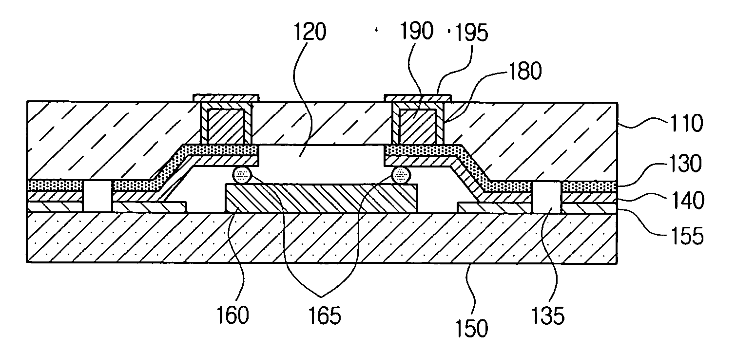
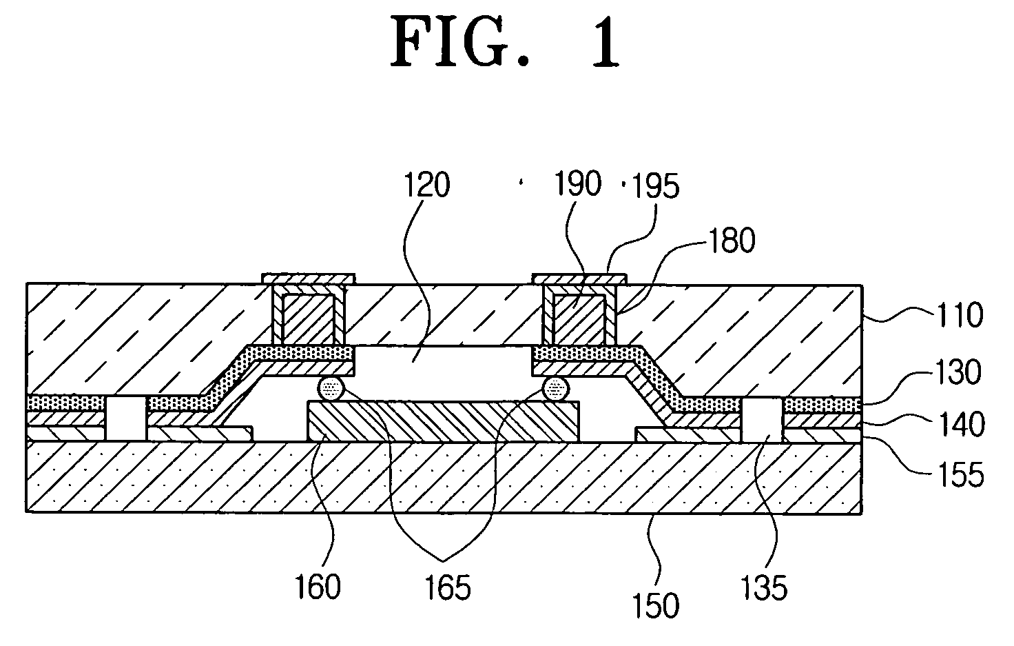
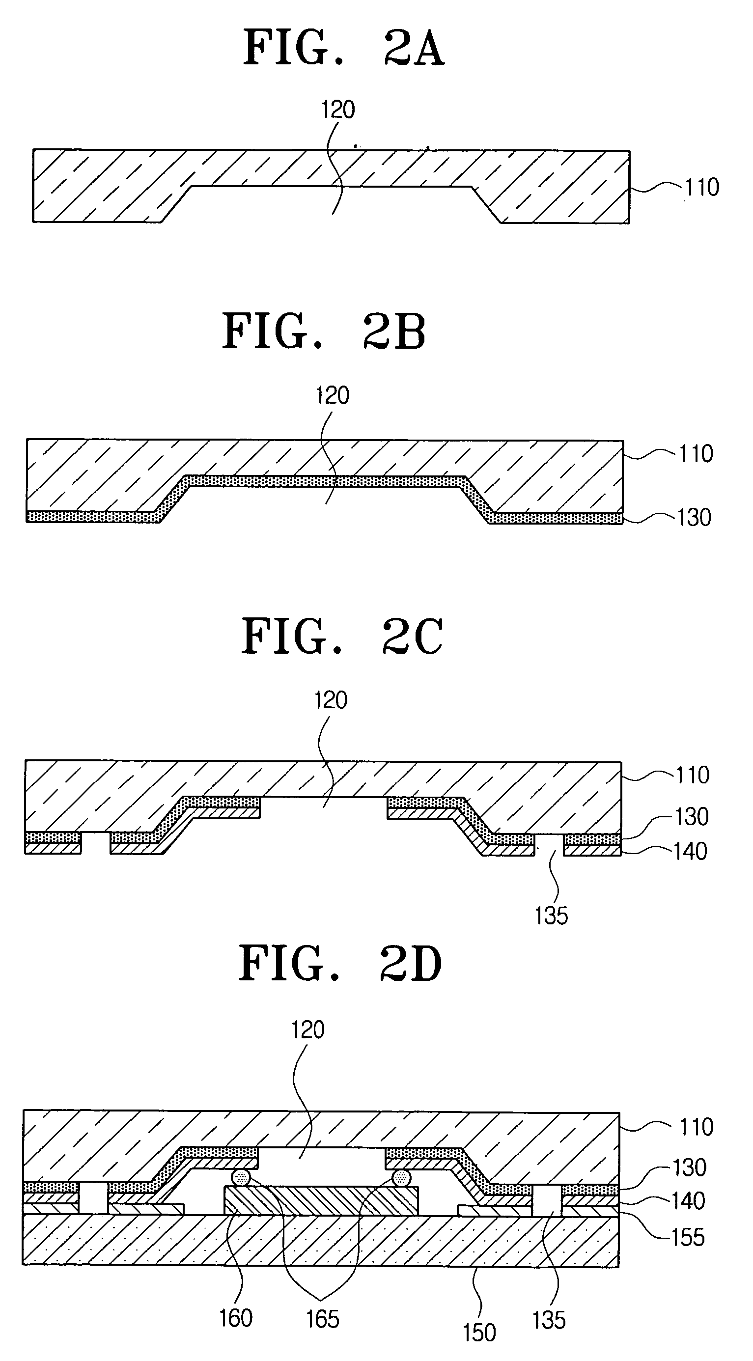
[0030]FIG. 1 is a cross-sectional view of a packaging chip according to an exemplary embodiment of the present invention. Referring to FIG. 1, the packaging chip includes a packaging wafer 110, a cavity 120, a metal layer 130, a under bump metallurgy layer (UBM) layer 140, a base wafer 150, a bonding layer 155, a ...


PUM


Abstract

A packaging chip in which a circuit module is packaged and a method of packaging a circuit module are provided. The packaging chip includes a base wafer; a circuit module on the base wafer; a packaging wafer having a cavity and combined with the base wafer so that the circuit module fits inside the cavity; a connecting electrode connecting upper and lower surfaces of the cavity; and a seed layer between the connecting electrode and the packaging wafer. The method includes etching a lower surface of the packaging wafer to form a cavity, stacking a metal layer in an area of the lower surface, combining the base wafer with the packaging wafer, polishing the packaging wafer, forming a viahole through the packaging wafer, stacking a seed layer on the packaging wafer, plating the inside of the viahole, removing the seed layer and forming an electrode.

Description

CROSS-REFERENCE TO RELATED APPLICATIONS [0001] This application claims the benefit of Korean Patent Application No. 2005-47854 filed Jun. 3, 2005, in the Korean Intellectual Property Office, the entire disclosure of which is incorporated herein by reference. BACKGROUND OF THE INVENTION [0002] 1. Field of the Invention [0003] The present invention relates to a packaging chip packaged by a packaging wafer and a method of manufacturing the packaging chip, and more particularly, to a packaging chip packaged using a packaging wafer including a seed layer stacked on an inner side of a viahole and a method of manufacturing the packaging chip. [0004] 2. Description of the Related Art [0005] Electronic packaging chips used in various electronic products include micro electronic circuits and thus may be damaged by external impacts. Thus, when such a packaging chip is manufactured, a packaging process must be performed to package the packaging chip so that the packaging chip has physical funct...

Claims


Application Information

Patent Timeline
Patent Type & Authority Applications(United States)
IPC IPC(8): H01L23/48
CPCH01L23/04H01L2224/16H01L27/14618H01L23/055H01L2224/73253H01L2924/15153H01L2924/15192
Inventor JUNG, KYU-DONGKIM, WOON-BAESONG, IN-SANGLEE, MOON-CHULHWANG, JUN-SIKHAM, SUK-JIN
Owner SAMSUNG ELECTRONICS CO LTD
Why Eureka
Try Eureka