Substrate structure of semiconductor package

a semiconductor and substrate structure technology, applied in semiconductor devices, semiconductor/solid-state device details, electrical apparatus, etc., can solve the problems of serious affecting the operation of the semiconductor chip, serious affecting the electronic performance and usage life, and increasing the heat generated by the semiconductor chip during operation, so as to reduce the production cost and simplify the manufacturing process , the effect of increasing the yield

a semiconductor and substrate structure technology, applied in semiconductor devices, semiconductor/solid-state device details, electrical apparatus, etc., can solve the problems of serious affecting the operation of the semiconductor chip, serious affecting the electronic performance and usage life, and increasing the heat generated by the semiconductor chip during operation, so as to reduce the production cost and simplify the manufacturing process , the effect of increasing the yield

US20060273458A1Inactive Publication Date: 2006-12-07PHOENIX PRECISION TECH CORP +1

Image

  • Substrate structure of semiconductor package
  • Substrate structure of semiconductor package
  • Substrate structure of semiconductor package

Examples


Embodiment Construction

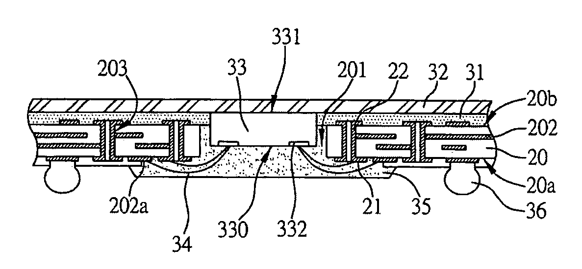
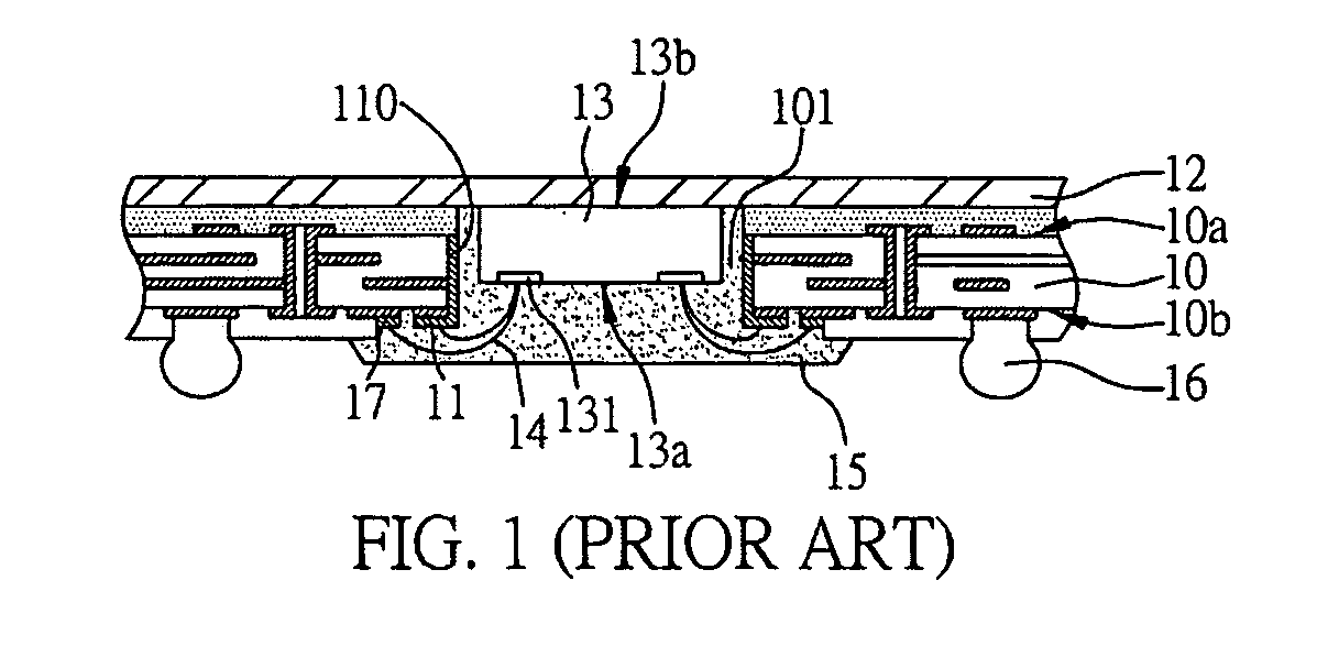
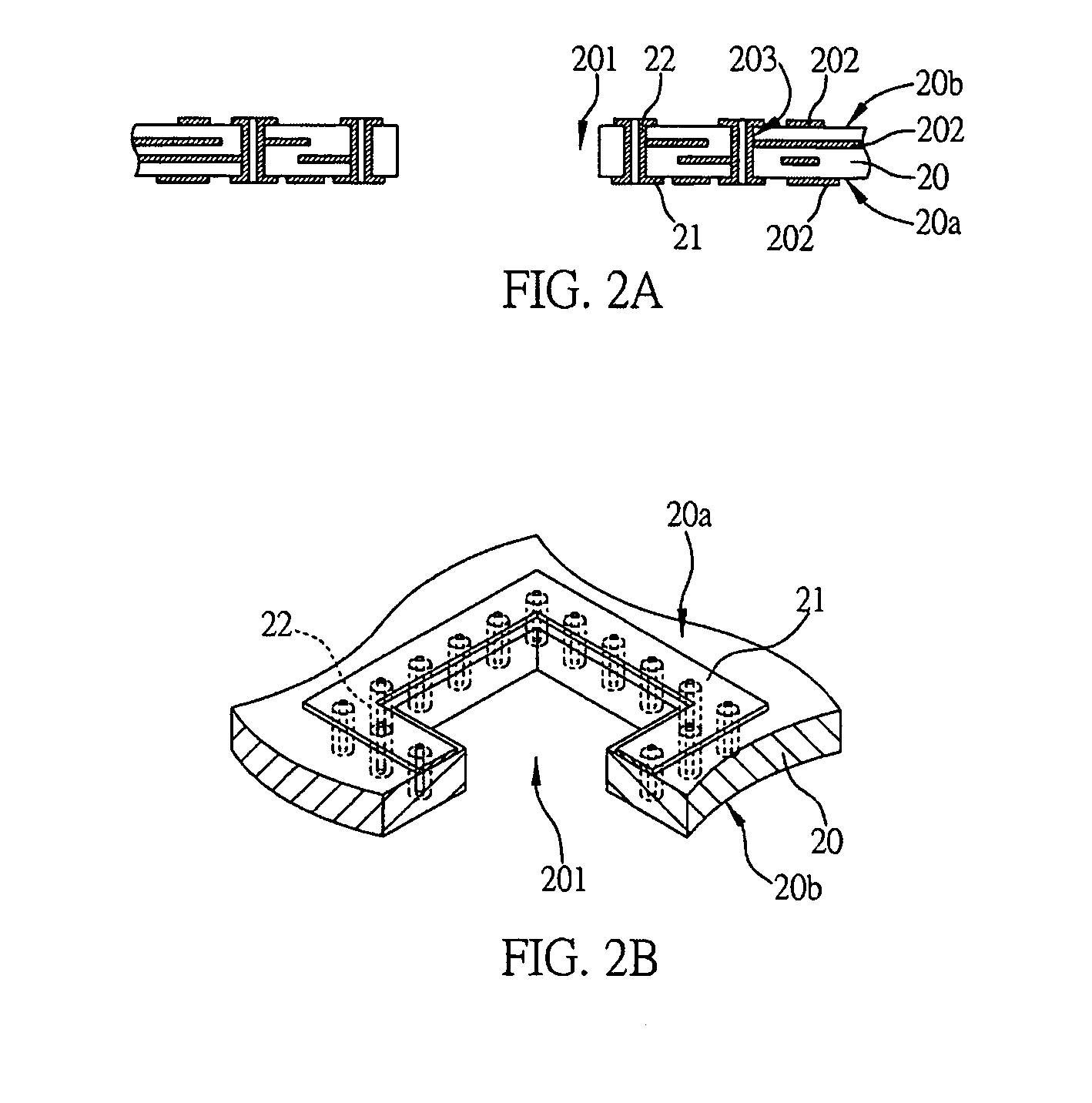
[0021] The present invention relates generally to substrate structures of semiconductor packages, and more particularly to a substrate structure of a cavity-down ball grid array (CDBGA) package. The following description is presented to enable one of ordinary skill in the art to make and use the invention and is provided in the context of a patent application and its requirements. Various modifications to the preferred embodiments and the generic principles and features described herein will be readily apparent to those skilled in the art. Thus, the present invention is not intended to be limited to the embodiments shown, but is to be accorded the widest scope consistent with the principles and features described herein.

[0022] The present invention is described in the following with specific embodiments, so that one skilled in the pertinent art can easily understand other advantages and effects of the present invention from the disclosure of the invention. The present invention may...


PUM


Abstract

A substrate structure of a semiconductor package is proposed. The structure includes a substrate with at least one opening; a grounding ring formed on the substrate and around the opening; and a plurality of plating through holes (PTH) formed in the substrate and corresponding to the grounding ring. The grounding area is increased by the grounding ring, so that the grounding quality of the substrate in package is improved. Meanwhile, it also simplifies the process, increases process yield and reduces cost of the process.

Description

CROSS-REFERENCE TO RELATED APPLICATIONS [0001] This application claims benefit under 35 USC 119 of Taiwan Application No. 094118705, filed on Jun. 7, 2005. FIELD OF THE INVENTION [0002] The present invention relates to substrate structures of semiconductor packages, and more particularly to a substrate structure of a cavity-down ball grid array (CDBGA) package. BACKGROUND OF THE INVENTION [0003] As the electronic industry continues to grow rapidly, electronic products have gradually moved to the direction of multi-functionality and high performance. However, as the semiconductor packages move to the direction of highly integration and miniaturization, generated heat from the semiconductor chip during operation increases dramatically. If the generated heat from the semiconductor chip cannot be readily dissipated, the electronic performance and usage lifetime would be seriously impaired. Moreover, as typical semiconductor devices usually lack of shielding, the semiconductor device may...

Claims


Application Information

Patent Timeline
07 Dec 2006
Publication
US20060273458A1
IPC
H01L23/48
CPC
H01L23/36; H01L2224/83; H01L23/49816; H01L23/49838; H01L23/50; H01L23/552; H01L2224/48091; H01L2224/48227
Inventors
HUANG, WEN-SHIEN; CHOU, E-TUNG