Surface acoustic wave device and method of manufacturing the same

a surface acoustic wave and acoustic wave technology, applied in piezoelectric/electrostrictive/magnetostrictive devices, piezoelectric/electrostriction/magnetostriction machines, electrical apparatus, etc., can solve problems such as voids generated in interdigital transducers, and achieve the effects of reducing the loss of insertion elements, and improving the properties of surface acoustic wav

Active Publication Date: 2006-12-07
QORVO US INC
View PDF14 Cites 23 Cited by
  • Summary
  • Abstract
  • Description
  • Claims
  • Application Information

AI Technical Summary

Benefits of technology

[0045] In addition, according to the invention, since the main electrode layer having a face-centered cubic crystal structure is laminated on the first base layer having rock-salt crystal structure or a face-centered cubic crystal structure such that a {111} plane, which is a closest-packed plane, has a constant gradient with respect to a surface of the piezoelectric substrate, it is possible to suppress the electromigration or the stress migration. As a result, since a breakage of electrodes and electrical breaks can be prevented, an insertion loss of elements can be decreased, and a Q-factor of resonators can be increased, the properties of the surface acoustic wave device can be improved.
[0046] Furthermore, according to the invention, since the {111} plane, which is a closest-packed plane, crosses the amplitude direction of SH waves if the {111} plane of the main electrode layer is parallel to the X axis of crystals of the piezoelectric substrate, the resistance to the electromigration or the stress migration can be improved.
[0047] In addition, according to the invention, since the main electrode layer can have a twin crystal structure of which a crystal grain boundary is linear if the film thickness of the second base layer is within a range of 0.5 to 10 nm, the power resistance of the surface acoustic wave device can be improved.
[0048] In addition, according to the invention, since the first base layer and second base layer are provided between the interdigital transducer portion and the piezoelectric substrate, it is possible to prevent the voids from being generated even though the temperature of the thermal treatment is high.
[0049] Since it is possible to raise the temperature of the thermal treatment, it is possible to reduce the variations even more in the serial resonance frequency and the parallel resonance frequency due to the temperature change of the surface acoustic wave device and to further improve the Q-factor of the surface acoustic wave device.
[0050] Further, since it is possible to raise the temperature of the thermal treatment, the film thickness of the insulating layer can be made large. By making the film thickness of the insulating layer large, it is possible to reduce the variations even more in the serial resonance frequency and the parallel resonance frequency due to the temperature change of the surface acoustic wave device and to further improve the Q-factor of the surface acoustic wave device.

Problems solved by technology

However, in the case of the configuration in which the interdigital transducers and the piezoelectric substrate are covered with the silicon oxide layer, a problem occurs in that voids are generated in the interdigital transducers.

Method used


Image

  • Surface acoustic wave device and method of manufacturing the same
  • Surface acoustic wave device and method of manufacturing the same
  • Surface acoustic wave device and method of manufacturing the same

Examples


first example

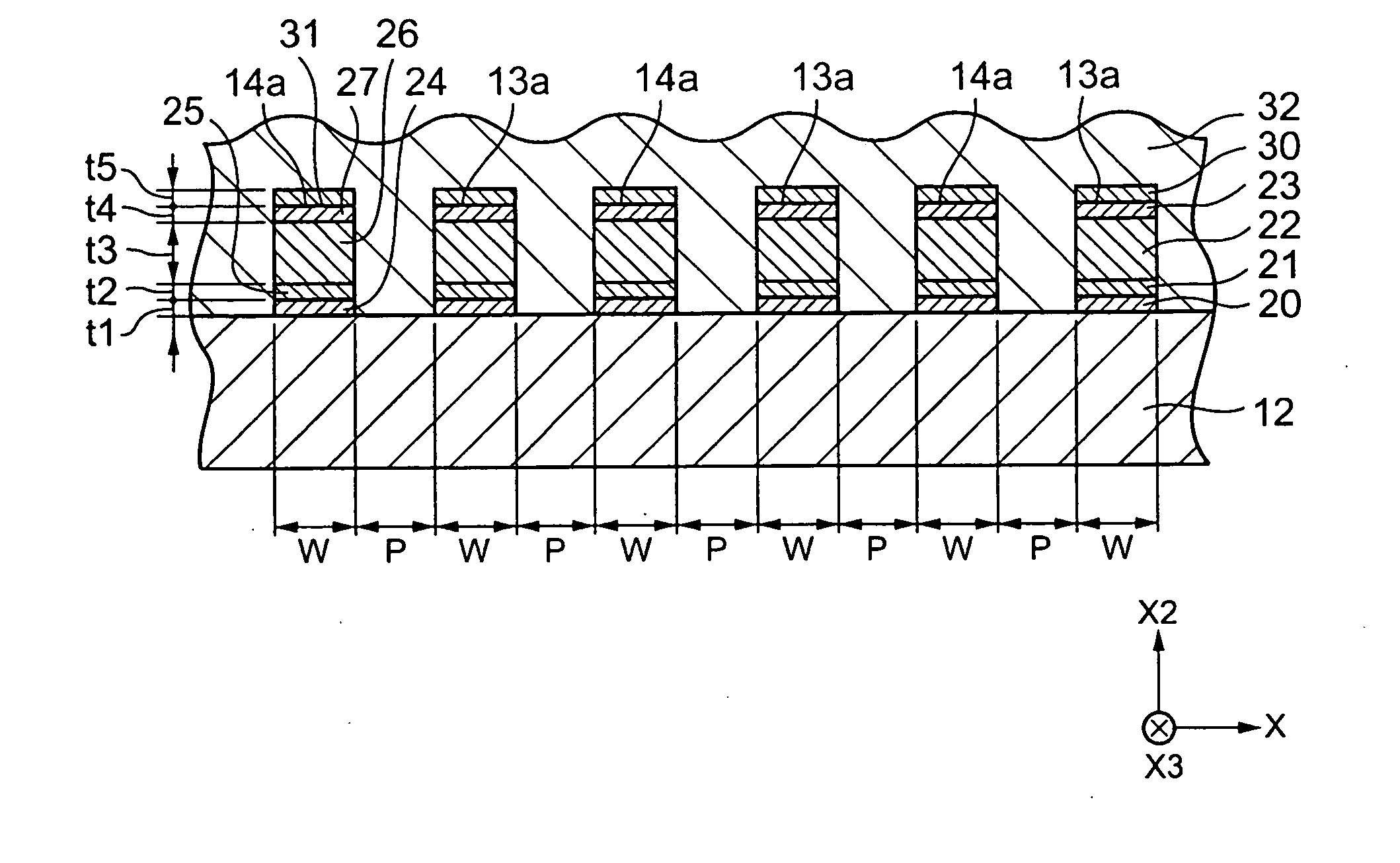
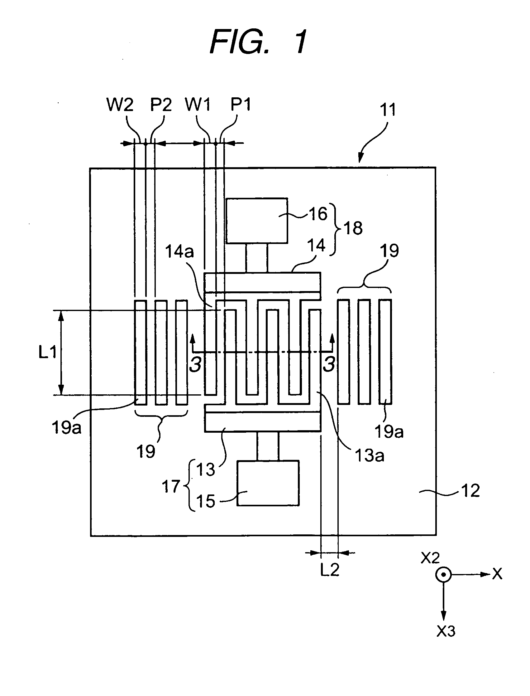
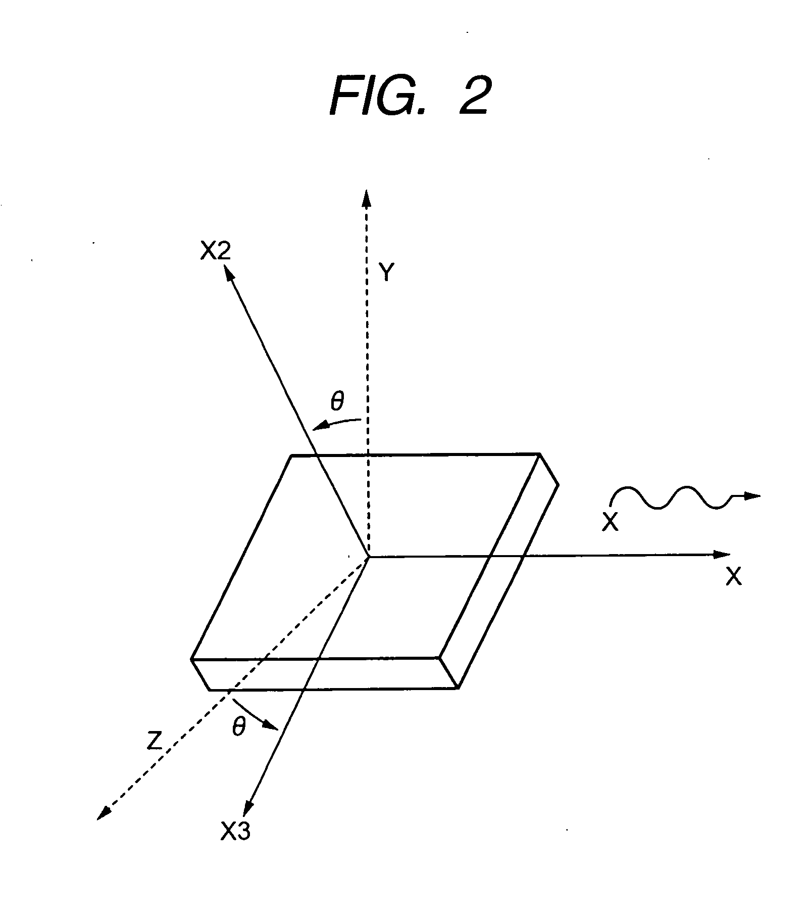
[0118] The Cu alloy layer (main electrode layer) made of CuAg alloy is formed on the piezoelectric substrate made of LiTaO3 having a Y-cut angle of 46° with a base layer interposed therebetween by using the sputtering method. FIG. 5 is an expanded photograph of the interdigital transducer portion of the surface acoustic wave device according to a first example in which a base layer is formed by laminating the first base layer made of TiN and the second base layer made of Cr, as viewed from a cross section orthogonal to the X axis of the LiTaO3 substrate. FIG. 6 is a partial side view schematically illustrating a part of the interdigital transducer portion shown in FIG. 5.

[0119] The film thickness of the first base layer (TiN) is 5 nm, the film thickness of the second base layer (Cr) is 2 nm, the film thickness of the Cu alloy layer (CuAg) is 80 nm, the film thickness of the first protective layer (TiN) is 5 nm, and the film thickness of the second protective layer (Cr) is 5 nm. The...

second example

[0122] The first base layer made of TiN, the second base layer made of Cr, the Cu alloy layer (main electrode layer) made of CuAg alloy, the first protective layer made of TiN, and the second protective layer made of Cr are formed on the piezoelectric substrate made of LiTaO3 having a Y-cut angle of 46° by using the sputtering method, and patterns of the interdigital transducer portion, the connection electrode portion, and the reflective electrode portion are formed. In addition, a curing process is performed at the temperature of 450° C and under atmosphere of oxygen (O2) and moisture (H2O) for thirty minutes.

[0123] The interdigital transducer portion includes the first base layer (TiN; 5 nm), the second base layer (Cr; X nm), the Cu alloy layer (CuAg; 80 nm), the first protective layer (TiN; 5 nm), and the second protective layer (Cr; 5 nm). The numbers in the parentheses are the film thicknesses, respectively.

[0124]FIG. 7 is an expanded photograph of the surface acoustic wave ...


PUM


Abstract

First base layers made of TiN or TiOxNy (where, 0<x<0.2, x+y=1) and second base layers made of Cr are provided between interdigital transducer portions and a piezoelectric substrate, and accordingly, it is possible to prevent voids from being generated in the interdigital transducer portions, which improves a power resistance of the surface acoustic wave device. In addition, since it is possible to prevent the voids from being generated in the interdigital transducer portions, it is possible to suppress the resistance of the interdigital transducer portions from increasing, which can reduce the loss of power. In addition, it is also possible to reduce the variations in a serial resonance frequency and a parallel resonance frequency.

Description

BACKGROUND OF THE INVENTION [0001] 1. Field of the Invention [0002] The present invention relates to a surface acoustic wave device having an electrode structure that can withstand high power at a high frequency band and a method of manufacturing the same. [0003] 2. Description of the Related Art [0004] Surface acoustic wave devices are electronic components using surface acoustic waves which are propagated in a state in which mechanical vibration energy is concentrated around only surfaces of solid substances, and are used for filters, resonators, duplexers, etc. [0005] In recent years, the trend in mobile communication terminals, such as mobile phones, are rapidly becoming smaller in size and lighter. For this reason, electronic components mounted on such mobile communication terminals should also be reduced in size. [0006] A surface acoustic wave device has a configuration in which a pair of interdigital transducers (IDT electrodes) made of a conductive material is disposed on a ...

Claims


Application Information

Patent Timeline
Patent Type & Authority Applications(United States)
IPC IPC(8): H03H9/25
CPCH03H3/08H03H9/14541H03H9/02929
Inventor FUJIMOTO, HARUHIKOOZAKI, KYOSUKEWAGA, SATOSHIMEGURO, TOSHIHIROIKEDA, TAKESHI
Owner QORVO US INC
Why Eureka
Try Eureka