Focus correction method for inspection of circuit patterns

a technology of circuit pattern and focus correction, which is applied in the direction of material analysis using wave/particle radiation, instruments, nuclear engineering, etc., can solve the problems of difficult focus correction based on image evaluation, and achieve the effects of reducing false information, reducing image sharpness, and stabilizing rejection ra

Inactive Publication Date: 2006-12-21
HITACHI HIGH-TECH CORP
View PDF10 Cites 87 Cited by
  • Summary
  • Abstract
  • Description
  • Claims
  • Application Information

AI Technical Summary

Benefits of technology

[0009] Accordingly, it is an object of this invention to prevent the reduction in rejection rate attributable to the out-of-focus condition due to the change in charge condition of the sample surface and reduce the false information thereby to improve the apparatus reliability.
[0011] According to this invention, the charge condition at a position preset in the repetitive pattern of the sample to be inspected is observed, the reduction in image sharpness attributable to the out-of-focus condition due to the charge is detected and a deflection lens is controlled by a preset correction value thereby to prevent the out-of-focus state during the inspection. By preventing the out-of-focus condition, the rejection rate is stabilized and the false information reduced for an improved apparatus reliability.

Problems solved by technology

The observation and inspection using the SEM poses the problem described below.
In the case where an image is acquired at a random position, on the other hand, the image evaluation is affected by the pattern and therefore the focus correction based on the image evaluation becomes difficult.

Method used


Image

  • Focus correction method for inspection of circuit patterns
  • Focus correction method for inspection of circuit patterns
  • Focus correction method for inspection of circuit patterns

Examples


Embodiment Construction

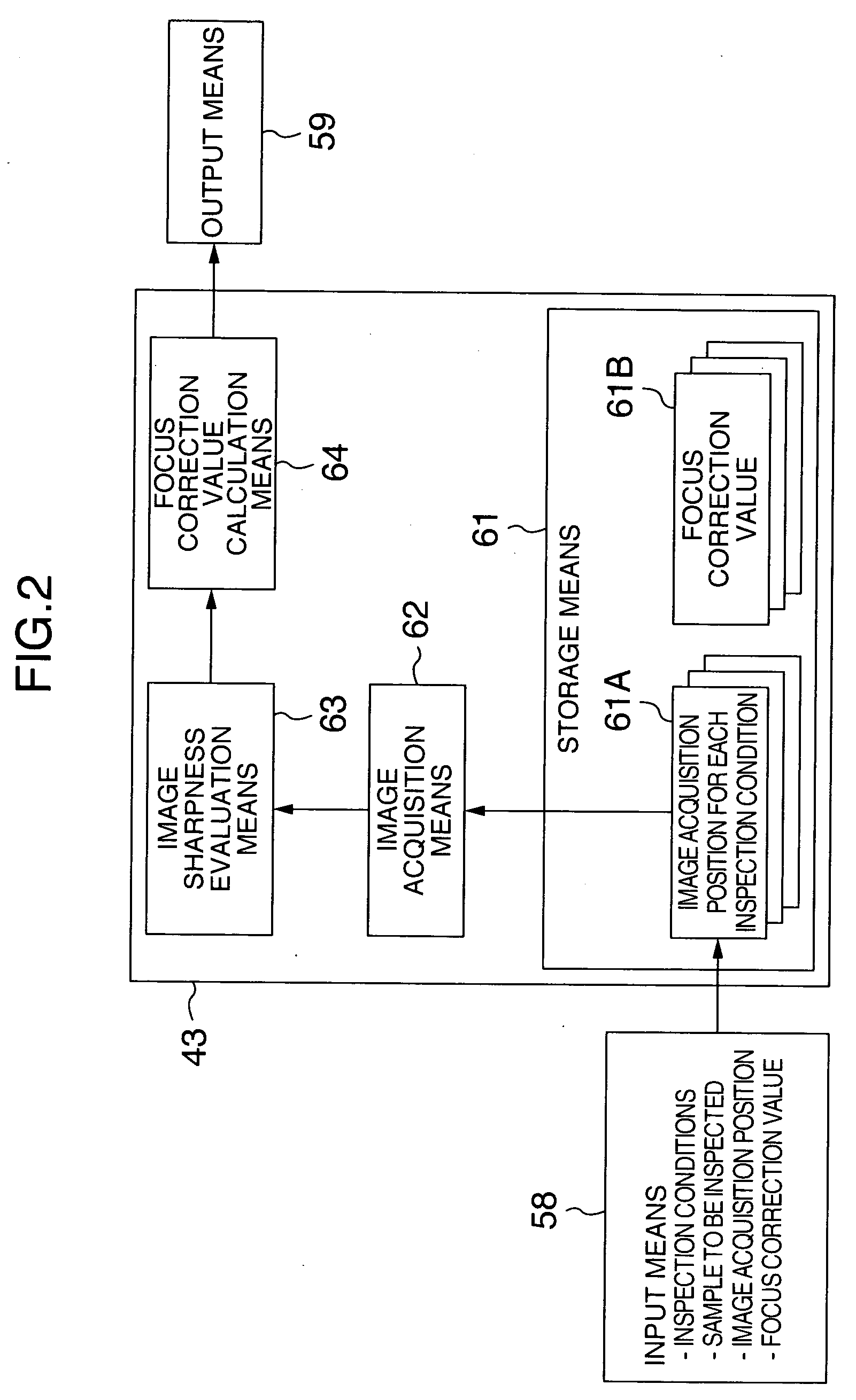
[0017] According to an embodiment of the invention, there are provided an apparatus and a method for inspecting the charged particle application circuit patterns, further including an image acquisition position storage means for storing a patterned image acquisition position in advance, wherein the sample charge condition is evaluated in accordance with the patterned image acquisition position so that the focal point is corrected by the focus control means.

[0018] An embodiment of the invention is explained below with reference to the drawings.

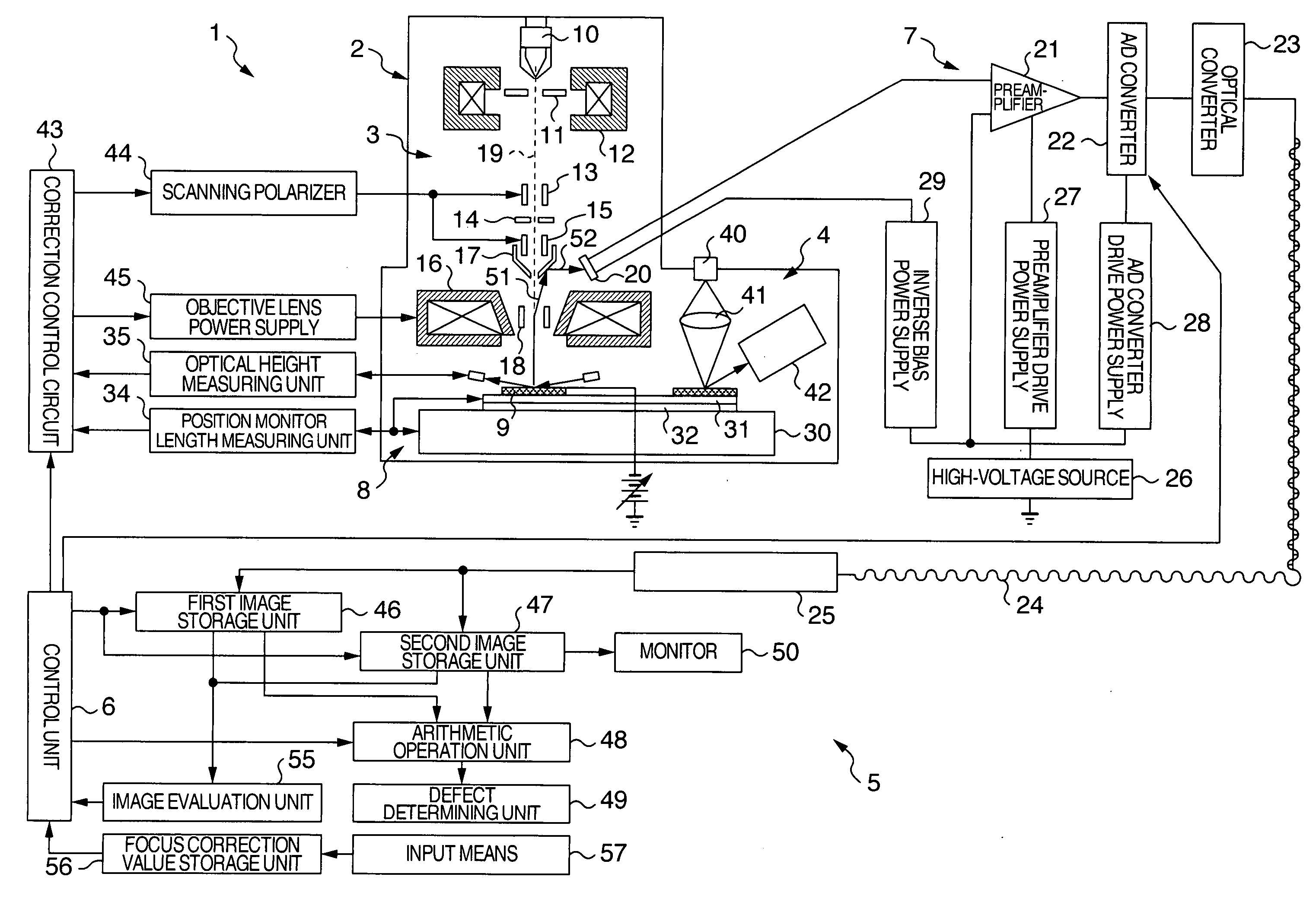
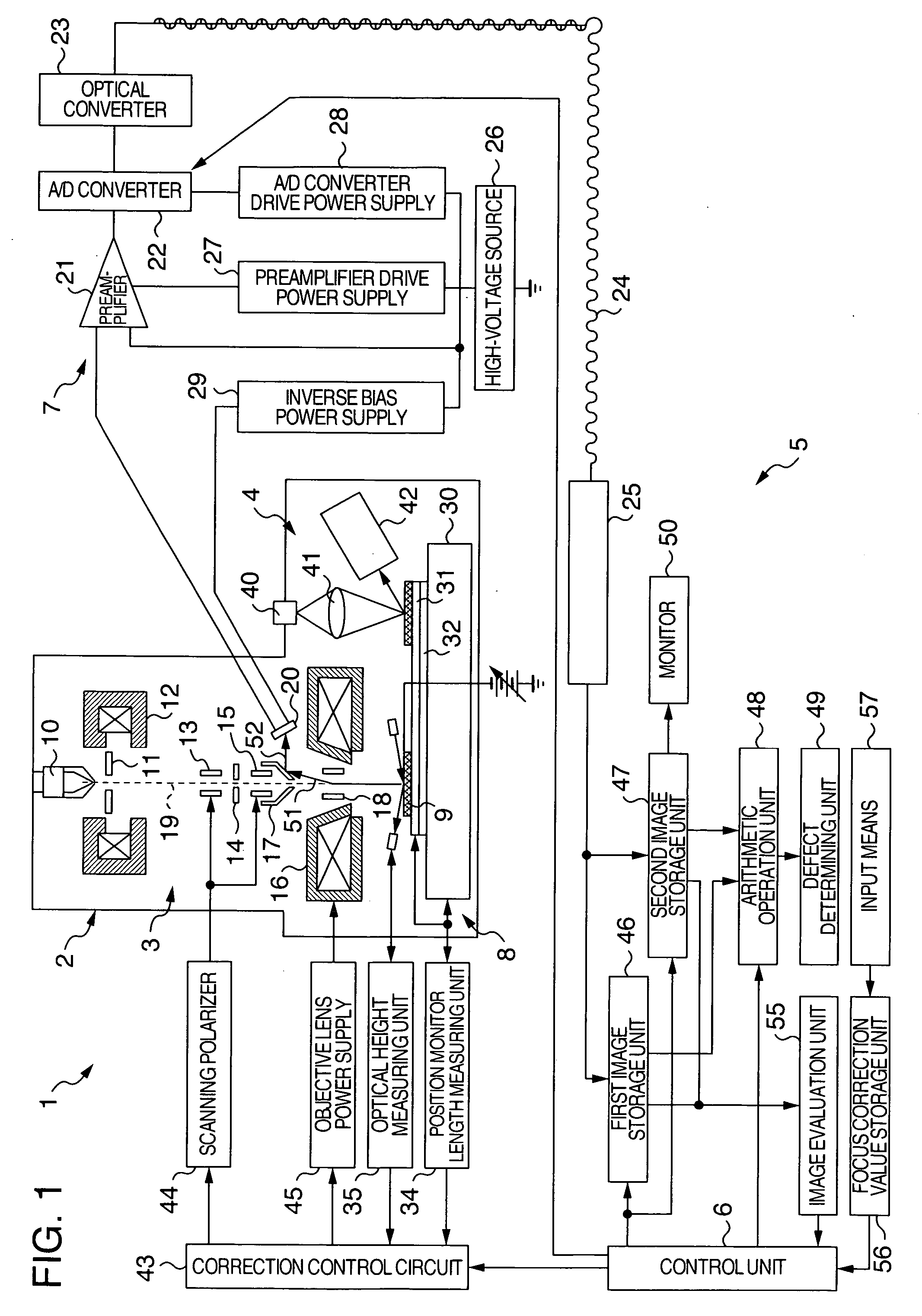
[0019] An example of the embodiment, of the invention is explained below with reference to FIG. 1. The configuration of a circuit pattern inspection apparatus 1 according to the embodiment of the invention is shown in FIG. 1. The circuit pattern inspection apparatus 1 includes an inspection room 2 exhausted into a vacuum and a spare room (not shown in this embodiment) for conveying a sample substrate (the substrate to be inspected, i.e. the s...


PUM


Abstract

A charged particle application circuit pattern inspection apparatus and method are disclosed, in which the reduction in the rejection rate attributable to an out-of-focus state due to the change in the charge condition on the sample surface is prevented and the false information is reduced to improve the apparatus reliability. The image acquisition position on a sample is stored in an image acquisition position storage unit, a focus correction value is stored in a focus correction value storage unit in accordance with the image acquisition position and the sample charge condition, the inspection conditions and the sample to be inspected are input from an input unit, the sample charge condition is evaluated in accordance with the image position acquisition position, and the focal point is corrected by a focus correction unit.

Description

BACKGROUND OF THE INVENTION [0001] This invention relates to an electron beam application circuit pattern inspection apparatus and an inspection method for inspecting a substrate having a fine circuit pattern such as a semiconductor device or a liquid crystal by electron beam radiation. [0002] The SEM pattern inspection apparatus using an electron beam finds wide applications for comparative inspection of the patterns formed on various substrates of various elements such as semiconductor elements. Especially, for lack of other proper means for observing and inspecting an arbitrary pattern several tens to several hundred nanometers in size, the SEM pattern inspection apparatus for observing and inspecting with an electron beam converged into as small a spot as possible is considered an important technique to observe and inspect the devices having the structure on the order of nanometer. [0003] To maintain a high accuracy of observation and inspection of a fine pattern, it is importan...

Claims


Application Information

Patent Timeline
Patent Type & Authority Applications(United States)
IPC IPC(8): G21K7/00
CPCH01J37/21H01J37/222H01J37/244H01J2237/2817H01J2237/004H01J2237/216H01J2237/2487H01J37/265
Inventor FUKUNAGA, FUMIHIKOHAYAKAWA, KOUICHITAKEDA, MASAYOSHI
Owner HITACHI HIGH-TECH CORP
Why Eureka
Try Eureka