Light emitting diode package with metal reflective layer and method of manufacturing the same

a technology of light-emitting diodes and reflective layers, which is applied in the direction of basic electric elements, electrical equipment, semiconductor devices, etc., can solve the problems of limiting automated manufacturing and mass production, low uniformity, and rather mediocre color development, so as to minimize irregular color distribution, small size, and easy manufacturing

Inactive Publication Date: 2006-12-21
SAMSUNG ELECTRO MECHANICS CO LTD
View PDF4 Cites 85 Cited by
  • Summary
  • Abstract
  • Description
  • Claims
  • Application Information

AI Technical Summary

Benefits of technology

[0013] Another object of certain embodiments of the invention is to provide an LED package having a metal reflective layer, which can be mass-produced without being affected by the LED chip size, and can be easily manufactured in a small size, and a method of manufacturing the same.
[0014] Further another object of certain embodiments of the invention is to provide an LED package having a metal reflective layer, whic

Problems solved by technology

However, in such a conventional structure, the LED chip 310 is formed in a recess 322 of the substrate, and a separate sealing plate 314 covers the recess 322, and thus limiting automated manufacturing and mass-production.
However, as an additional

Method used


Image

  • Light emitting diode package with metal reflective layer and method of manufacturing the same
  • Light emitting diode package with metal reflective layer and method of manufacturing the same
  • Light emitting diode package with metal reflective layer and method of manufacturing the same

Examples


Embodiment Construction

[0026] Preferred embodiments of the present invention will now be described in detail with reference to the accompanying drawings.

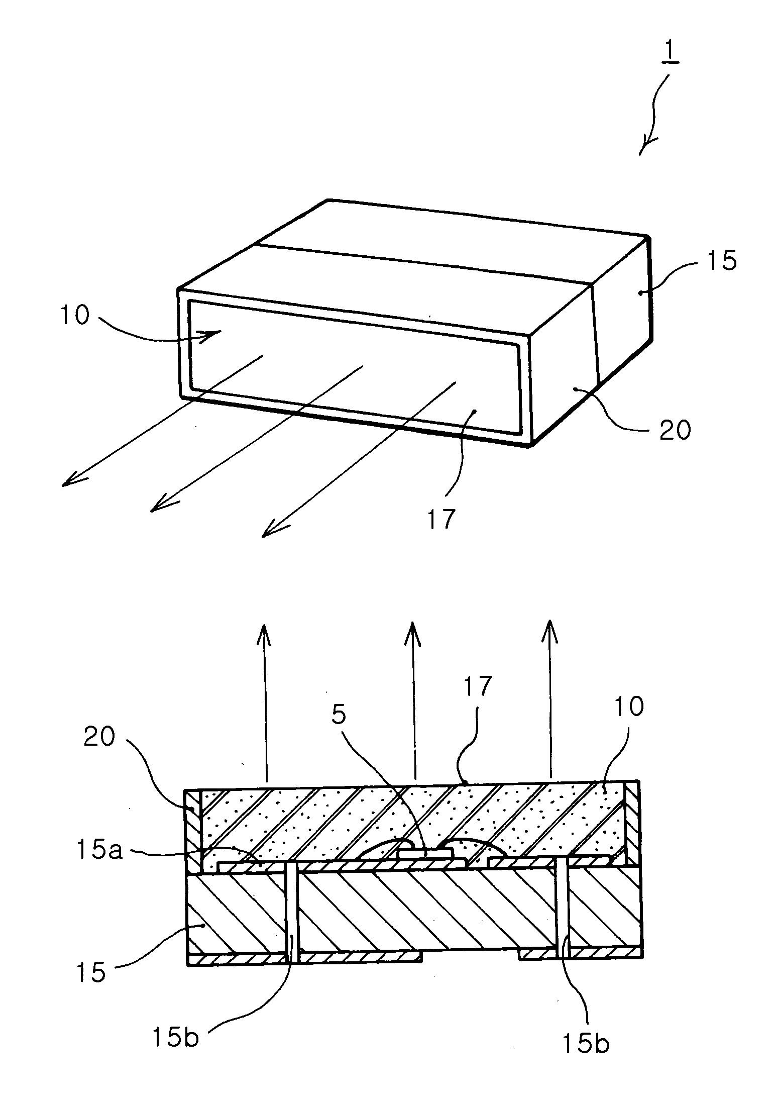
[0027] As shown in FIG. 4, an LED package 1 having a metal reflective layer according to the present invention is for emitting light from an LED chip 5 in one direction of an encapsulant 10.

[0028] Light is emitted through a light transmitting surface 17 which is preferably in front and in parallel with a plane where the LED chip 5 is disposed.

[0029] The LED package 1 having a metal reflective layer according to the present invention has a substrate with electrodes 15a and 15b formed thereon. The substrate 15 may preferably be a Printed Circuit Board (PCB) or a ceramic substrate having pattern electrodes 15a and vertical electrodes 15b such as vias.

[0030] In addition, an LED chip 5 is electrically connected to the electrode 15a and mounted on the substrate 15. The LED chip 5 may be a horizontal type with all of its electric terminals formed only on an ...


PUM


Abstract

The invention relates to an LED package having a metal reflective layer for focusing and emitting light through a side of the package, and a manufacturing method of the same. The LED package includes a substrate with an electrode formed thereon, a light emitting diode chip disposed on the substrate, and an encapsulant covering the LED chip and the substrate to protect the LED chip. The LED package also includes a metal reflective layer surrounding side surfaces of the encapsulant to form a light transmitting surface on a top surface of the encapsulant. The invention minimizes light loss, improves luminance, can be mass-produced as a PCB type, and adopts EMC transfer molding to minimize irregular color distribution, thereby improving optical quality.

Description

CLAIM OF PRIORITY [0001] This application claims the benefit of Korean Patent Application No. 2005-53163 filed on Jun. 20, 2005, in the Korean Intellectual Property Office, the disclosure of which is incorporated herein by reference. BACKGROUND OF THE INVENTION [0002] 1. Field of the Invention [0003] The present invention relates to a Light Emitting Diode (LED) package having a metal reflective layer for focusing and emitting light through one side of the package, and a method of manufacturing the same. More particularly, the invention relates to an LED package with a metal reflective layer minimized in light loss and improved in luminance, which can be mass-manufactured as a PCB type in a small size unaffected by the size of an LED chip, and is improved in productivity. [0004] 2. Description of the Related Art [0005] In general, a mobile phone or PDA adopts a light emitting diode (LED) package in various sizes for a backlight. [0006] As the backlights are becoming slimmer, the LED ...

Claims


Application Information

Patent Timeline
IPC IPC(8): H01L33/00H01L33/56H01L33/50H01L33/60H01L33/62
CPCH01L33/486H01L33/60H01L24/97H01L2224/48091H01L2224/48227H01L2224/48247H01L2924/12041H01L2224/73204H01L2924/00014H01L2924/00H01L2924/15787H01L2924/181
Inventor PARK, JUNG KYULEE, SEON GOOHAN, KYUNG TAEGHAN, SEONG YEON
Owner SAMSUNG ELECTRO MECHANICS CO LTD
Why Eureka
Try Eureka