Manufacturing method of light-collecting device, light-collecting device and phase shift mask
a technology of light-collecting devices and manufacturing methods, applied in the direction of magnification glasses, instruments, applications, etc., can solve the problems of inability to connect the light-transmitting portion and the phase-shift portion to each other, the fine-structured light-collecting device cannot be manufactured, and the difficulty of fine-processing, so as to facilitate fine processing and prevent the effect of deterioration of the characteristic due to lens distortion
- Summary
- Abstract
- Description
- Claims
- Application Information
AI Technical Summary
Benefits of technology
Problems solved by technology
Method used
Image
Examples
first embodiment
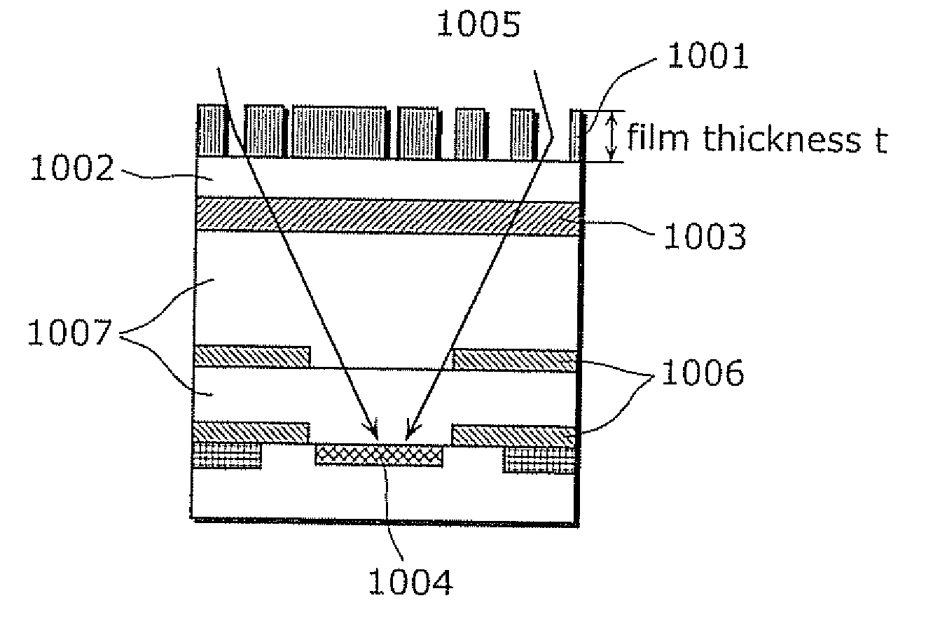
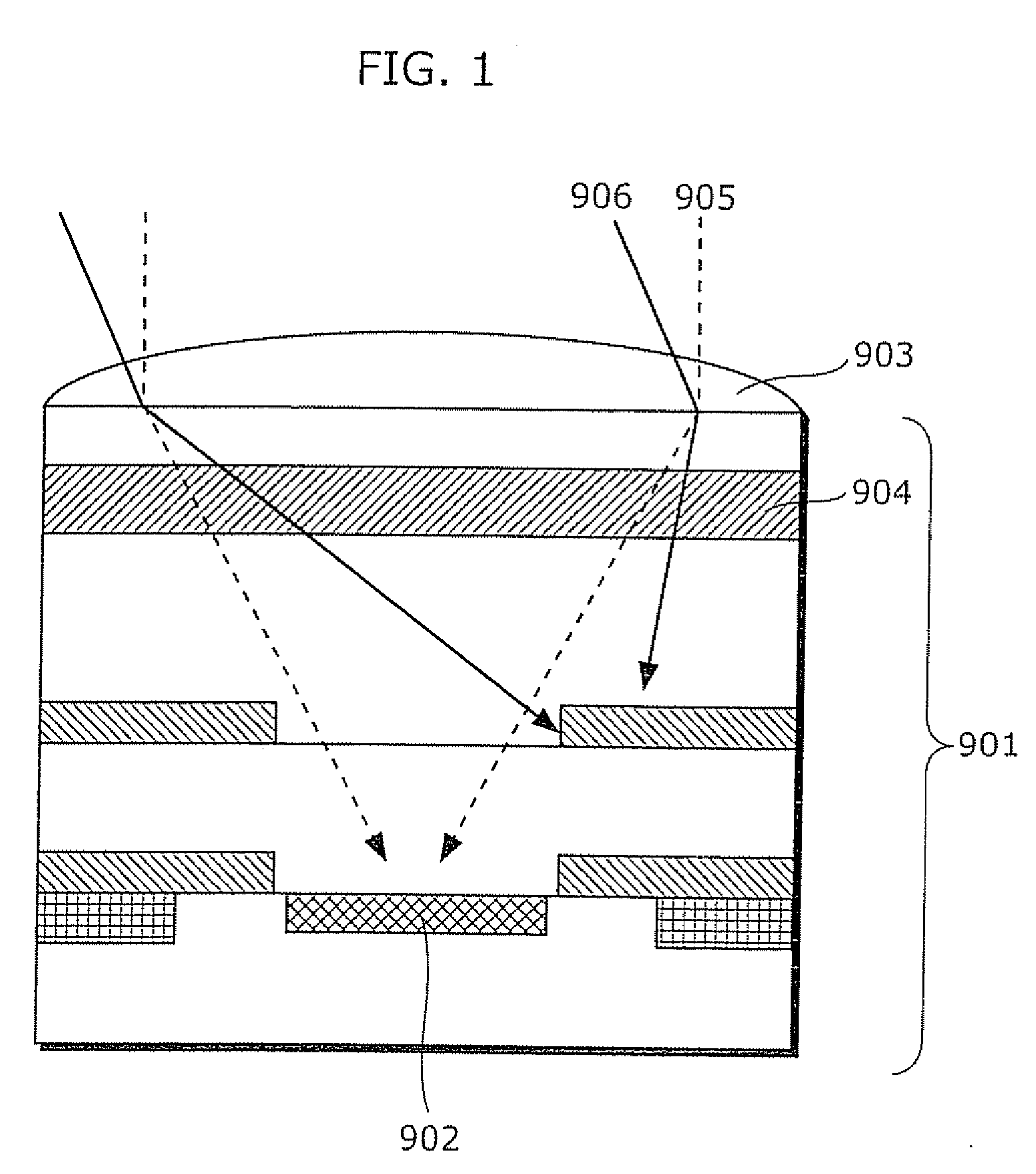
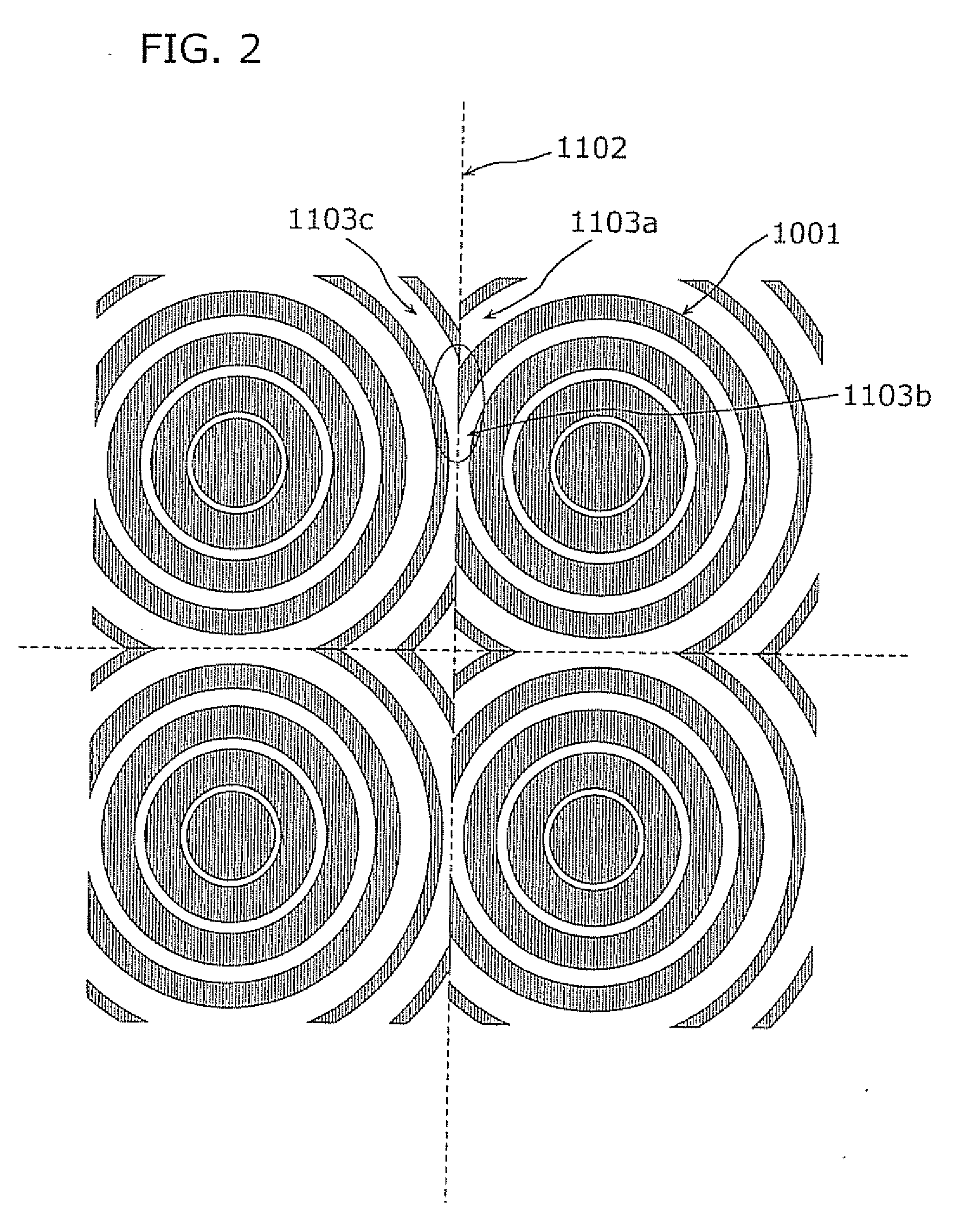
[0051]FIG. 3A is a diagram showing a cross-section of a pixel unit having a light-collecting device (a lens) according to the first embodiment. FIG. 3B shows a top view of the pixel unit. This pixel unit includes light-transmitting films 1001, a substrate 1002, a color filter 1003, a photodiode 1004, Aluminum wiring 1006, a planarized film 1007, and a frame 1008. The light-transmitting films 1001 have been processed into a substantially circle shape or a substantially concentric zone shape. A radial difference between adjacent zones (the perimeter of the light-transmitting film 1001 in FIG. 3B) is assumed to be a constant value. The width of a zone is as long as a wavelength of natural light. The width of a zone is typically as long as 0.1 μm. The refractive index of the incident light 1005 which passes through the respective light-transmitting films 1001 and a medium (typically, air) is a mean value between a value of the refractive index of the light-transmitting film 1001 and a v...
second embodiment
[0058] The following problem is found in the method of manufacturing the light-collecting device according to the aforementioned first embodiment. FIG. 6A is a diagram showing a shape of the photoresist 105, which is calculated by simulation, in the process shown in FIG. 4C according to the first embodiment of the present invention. In the diagram, white regions indicate where the photoresist 105 is to be remained and black regions indicate where the photoresist 105 is to be removed by development, seen from the top. In FIG. 6A, it is found that a portion corresponding to the peripheral light-blocking frames 104 of the pixel layout 108 cannot be formed precisely. In other words, whereas the light-blocking frames 104 are formed on the corners of the pixel layout 108, they are not formed in regions other than the corners. Therefore, it is assumed that the shape of the light-collecting device is distorted and the characteristics are deteriorated. Accordingly, in the second embodiment o...
third embodiment
[0062] The following problem is found in the method of manufacturing the light-collecting device according to the aforementioned second embodiment. FIG. 7A is a diagram showing a structure of a phase shift mask used for a method of manufacturing a light-collecting device according to the third embodiment of the present invention. The difference between the phase shift mask in FIG. 7A and the phase shift mask in FIG. 5 is that FIG. 5 shows a shape of light-collecting devices placed near the center of the imaging plane in which pixels are arranged in a matrix while FIG. 7A shows a shape of light-collecting devices placed in the periphery of the imaging plane. In other words, each of the light-collecting devices shown in FIG. 7A is placed being shifted toward the center of the imaging plane. This phase shift mask includes light-blocking portions 401, light-transmitting portions 402, phase shift portions 403 and light-blocking frames 404. The phase shift portions 403 are placed on both ...
PUM
 Abstract
Description
Claims
Application Information


