
Etching method and composition for forming etching protective layer

An etching protection and composition technology, which is applied to photosensitive materials for opto-mechanical equipment, photo-engraving processes for patterned surfaces, instruments, etc. Problems such as pattern-transferring shape deterioration, etc.

Inactive Publication Date: 2009-04-15
MERCK PATENT GMBH
View PDF8 Cites 0 Cited by
  • Summary
  • Abstract
  • Description
  • Claims
  • Application Information

AI Technical Summary

Problems solved by technology

The problem with these kinds of polymers is that their etch resistance is generally lower than that of the above-mentioned novolac resins, and requires etching conditions, especially an etching selectivity ratio between the resist film layer and the etched layer, that is, preferably Etching speed of each layer (slow for resist and fast for etched layers), and in turn, pattern-transfer shape deterioration after etching occurs
However, there is no suggestion in the patent publication to improve the etch resistance of the resist

Method used


Image

  • Etching method and composition for forming etching protective layer

Examples


reference example 1

[0030] (Formation of resist pattern)

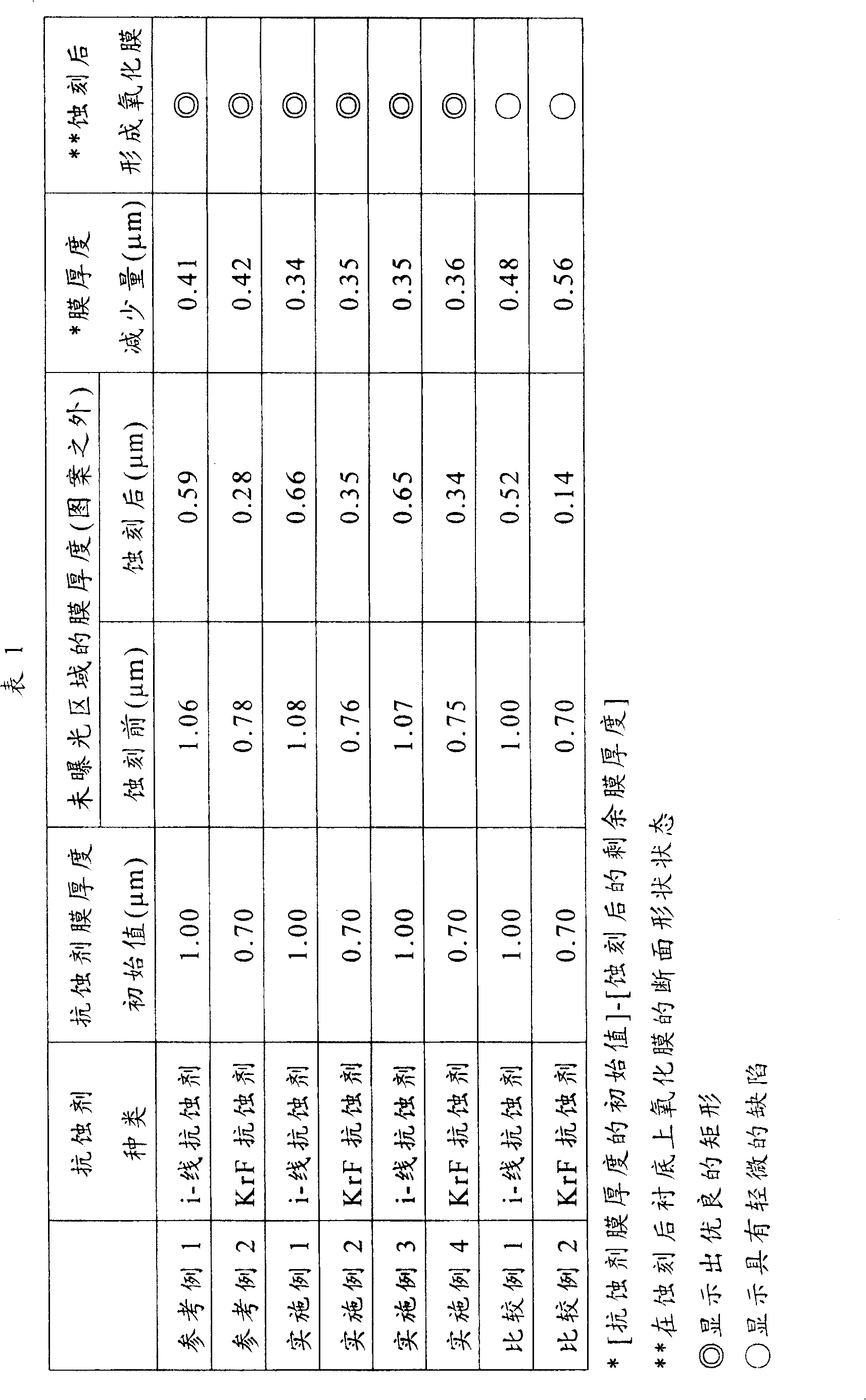
[0031] Positive photoresist AZ 7900 (i-line resist) ("AZ" is a registered trademark) produced by Clariant Japan K.K. was coated using a spin coater produced by Lithotech Japan Co., LARCULTIMA-1000 onto a 6-inch silicon wafer with a 1 μm oxide film and treated with HMDS. The coated silicon wafer was preheated on a heating plate at 100° C. for 60 seconds, and a resist film with a thickness of 1 μm was formed. The film thickness was measured by a film thickness measuring device produced by Dai-Nippon Screen Co. (Lambda Ace). Then, the silicon wafer is exposed, using a stepper (produced by Nikon Co., NSR 1755iB, NA=0.54) of i-line (365nm) exposure wavelength, through a reticle of a line and space pattern with a width of 0.3 μm. Change exposure in steps. The exposed silicon wafer was heated on a hot plate at 100° C. for 90 seconds. At 23°C, the silicon wafer was developed by paddle development for 1 minute, and AZ 300MIF Developer produced...

reference example 2

[0050] Using a spin coater (Mark 8) produced by Tokyo Electron Co., a positive-type photoresist (KrF resist) consisting of the composition described below was applied onto a 6-inch silicon wafer, which There is a 1μm oxide film and treated with HMDS. The coated silicon wafer was preheated on a heating plate at 90° C. for 60 seconds, and prepared to form a resist film with a thickness of 0.7 μm. The film thickness was measured by a film thickness measuring device produced by Dai-Nippon Screen Co. (Lambda Ace). Then, the silicon wafer was exposed, using a stepper with 248nm exposure wavelength (produced by Canon Co., FPA3000EX5, NA=0.63), and the exposure amount was changed step by step through a reticle with a line and space pattern of 0.3 μm width. The exposed silicon wafer was heated on a hot plate at 110° C. for 90 seconds. At 23°C, the silicon wafer was developed by paddle development for 1 minute, and AZ 300MIF Developer produced by Clariant Japan K.K. was used as an alk...

Embodiment 1

[0058] An etching mask having an etching protective layer was formed in the same manner as in Reference Example 1 except that Composition B for forming an etching protective layer prepared as described below was used instead of Composition A for forming an etching protective layer. Etching was performed on a substrate having an etching mask in the same manner as in Reference Example 1, and the etching resistance of the resist mask was evaluated. The results are shown in Table 1.

[0059] (Preparation of composition B for forming an etch protection layer)

[0060] Mix each of the components described below in the proportions described below, stir well and dissolve. Composition B for forming an etching protective layer was prepared after filtering the composition through a 0.2 μm filter.

[0061] Component Parts by weight

[0062] Copolymer of acrylic acid and p-hydroxystyrene (85 / 15 molar ratio) 2.0

[0063] Methoxymethylated melamine 0.5

[0064] 2-propanol 2.5

[0065] ...


PUM

PropertyMeasurementUnit
molecular weightaaaaaaaaaa
weight-average molecular weightaaaaaaaaaa
molecular weightaaaaaaaaaa

Abstract

This invention offers a method to improve etching resistance of etching mask upon etching comprising steps of forming a pattern on a substrate by using photoresist, applying a composition for forming an etching protection layer containing water-soluble or water-dispersible resin, crosslinking agent and water and / or water-soluble organic solvent as a solvent, forming etching protection layer which is insoluble in a developer containing water in the interface between a composition for forming an etching protection layer and a photoresist by heating, removing by a developer unnecessary area excluding etching protection layer made of a composition for forming an etching protection layer, and treating a substrate by etching using photoresist pattern as a mask.

Description

technical field [0001] The present invention relates to an etching method of a substrate, and the etching resistance can be improved by using an etching mask made of a resist and a composition for forming an etching protection layer. In more detail, the present invention relates to a method for improving etching resistance of etching masks used for producing semiconductor devices, forming liquid crystal display (LCD) panels of liquid crystal display devices, producing circuit substrates such as thermal heads, and the present invention also relates to It relates to a method of etching a substrate using the etching mask, which improves the etching resistance, and to a composition for forming an etching protection layer, which improves the etching resistance of a resist pattern. Background technique [0002] In a wide range of processes for producing semiconductor integrated circuits such as LSI, liquid crystal display panels for liquid crystal display devices, producing circui...

Claims


Application Information

Patent Timeline
Patent Type & Authority Patents(China)
IPC IPC(8): G03F7/11G03F7/40H01L21/027H01L21/306C23F1/00G03F7/00H01L21/308H01L21/311H01L21/3213
CPCH01L21/32139H01L21/3081H01L21/31144H01L21/0274G03F7/40H01L21/302
Inventor 田中初幸
Owner MERCK PATENT GMBH
Learn More