Multilayer electronic component and multilayer ceramic capacitor

a multi-layer ceramic capacitor and electronic component technology, applied in the direction of capacitors, fixed capacitor details, stacked capacitors, etc., can solve the problems of failure to achieve sufficient sintering of the outer multi-layer portions, baking unevenness and uneven baking in the multi-layer electronic components. to inhibit the occurrence of cracks and inhibit baking unevenness

Inactive Publication Date: 2006-12-21
TDK CORPARATION
View PDF10 Cites 7 Cited by
  • Summary
  • Abstract
  • Description
  • Claims
  • Application Information

AI Technical Summary

Benefits of technology

[0012] When a ceramic layer is made to contain a glass component, it becomes feasible to lower the sintering temperature in the ceramic layer. In the ceramic layer, the sintering temperature decreases with increase in the component amount ratio of the amount of the glass component in the ceramic layer to the amount of the principal component of the ceramic layer. In this multilayer electronic component, the component amount ratio of the second ceramic layers is larger than the component amount ratio of the first ceramic layers, so that the sintering temperature of the second ceramic layers is lower than the sintering temperature of the first ceramic layers. It is considered on the other hand that the first ceramic layers alternately laminated with the internal circuit element conductors are affected by the internal circuit element conductors to substantially lower the sintering temperature. It results in decreasing the sintering temperature both in the inner multilayer portion and in the outer multilayer portions and thus decreasing the difference of sintering temperatures between the inner multilayer portion and the outer multilayer portions. For this reason, it becomes feasible to inhibit the baking unevenness in this multilayer electronic component. The decrease in the difference of sintering temperatures between the inner multilayer portion and the outer multilayer portions decreases a shrinkage ratio difference between the inner multilayer portion and the outer multilayer portions and also suppresses occurrence of cracks. In this multilayer electronic component, the outer multilayer portions can be sufficiently sintered even if the baking is carried out in accordance with the sintering temperature of the inner multilayer portion. This enables improvement in reliability of the multilayer electronic component.
[0014] When the inner multilayer portion has the third ceramic layer formed so as to absorb the level difference due to the thickness of the internal circuit element conductor, occurrence of delamination is inhibited in this multilayer electronic component. Since the component amount ratio of the third ceramic layer is larger than the component amount ratio of the first ceramic layers, it becomes feasible to inhibit the baking unevenness in the inner multilayer portion.
[0015] Preferably, a rate of the component amount ratio of the first ceramic layers to the component amount ratio of the second ceramic layers is not less than 0.5, and less than 1.0. When the rate of the component amount ratio of the first ceramic layers to the component amount ratio of the second ceramic layers is within this range, the difference of shrinkage ratios between the inner multilayer portion and the outer multilayer portions can be reduced, so as to inhibit occurrence of cracks.
[0018] In this multilayer ceramic capacitor, the difference of sintering temperatures between the outer multilayer portions and the inner multilayer portion can be decreased and the baking unevenness can be inhibited.

Problems solved by technology

The Inventors found that baking of this multilayer electronic component resulted in sintering the inner multilayer portion at lower temperatures than those for the outer multilayer portions and, in turn, causing the baking unevenness in the multilayer electronic component.
The aforementioned baking unevenness occurs not only with baking at a temperature suitable for the inner multilayer portion, but also with baking at a temperature suitable for the outer multilayer portions.
Namely, the baking at the temperature suitable for the inner multilayer portion leads to failure in sufficient sintering of the outer multilayer portions.
On the other hand, the baking at the temperature suitable for the outer multilayer portions leads to excessive baking of the inner multilayer portion.
If the inner multilayer portion is excessively baked, there will arise a problem that the ceramic layers of the inner multilayer portion turn into a semiconductor and a problem that the internal circuit element conductors turn into spheroidized to lower the coverage.

Method used


Image

  • Multilayer electronic component and multilayer ceramic capacitor
  • Multilayer electronic component and multilayer ceramic capacitor
  • Multilayer electronic component and multilayer ceramic capacitor

Examples


Embodiment Construction

[0025] Preferred embodiments of the present invention will be described below in detail with reference to the accompanying drawings. In the description, identical elements or elements with identical functionality will be denoted by the same reference symbols, without redundant description.

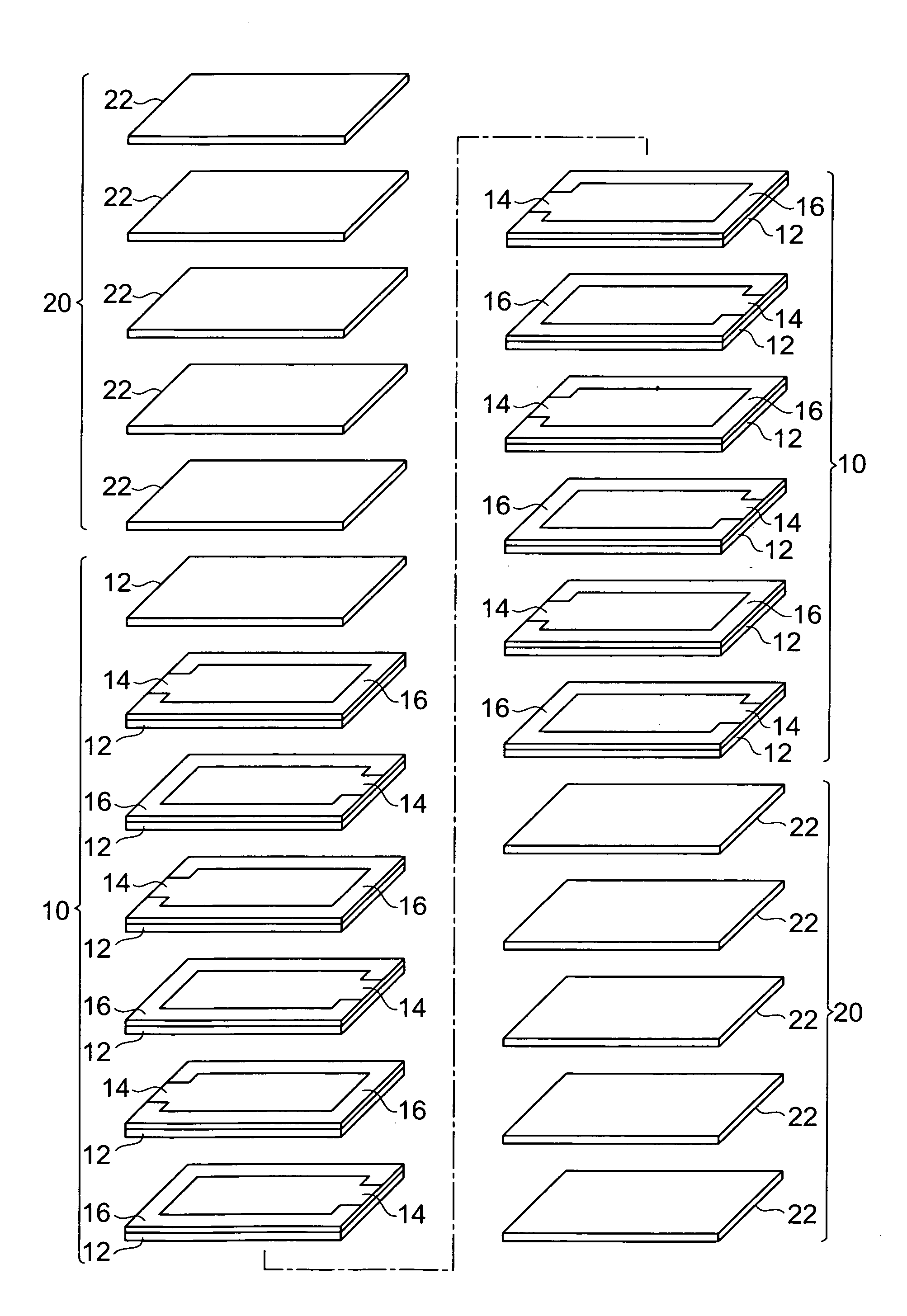
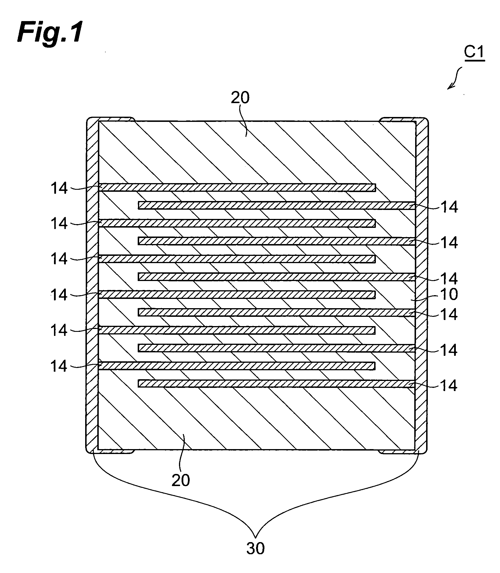
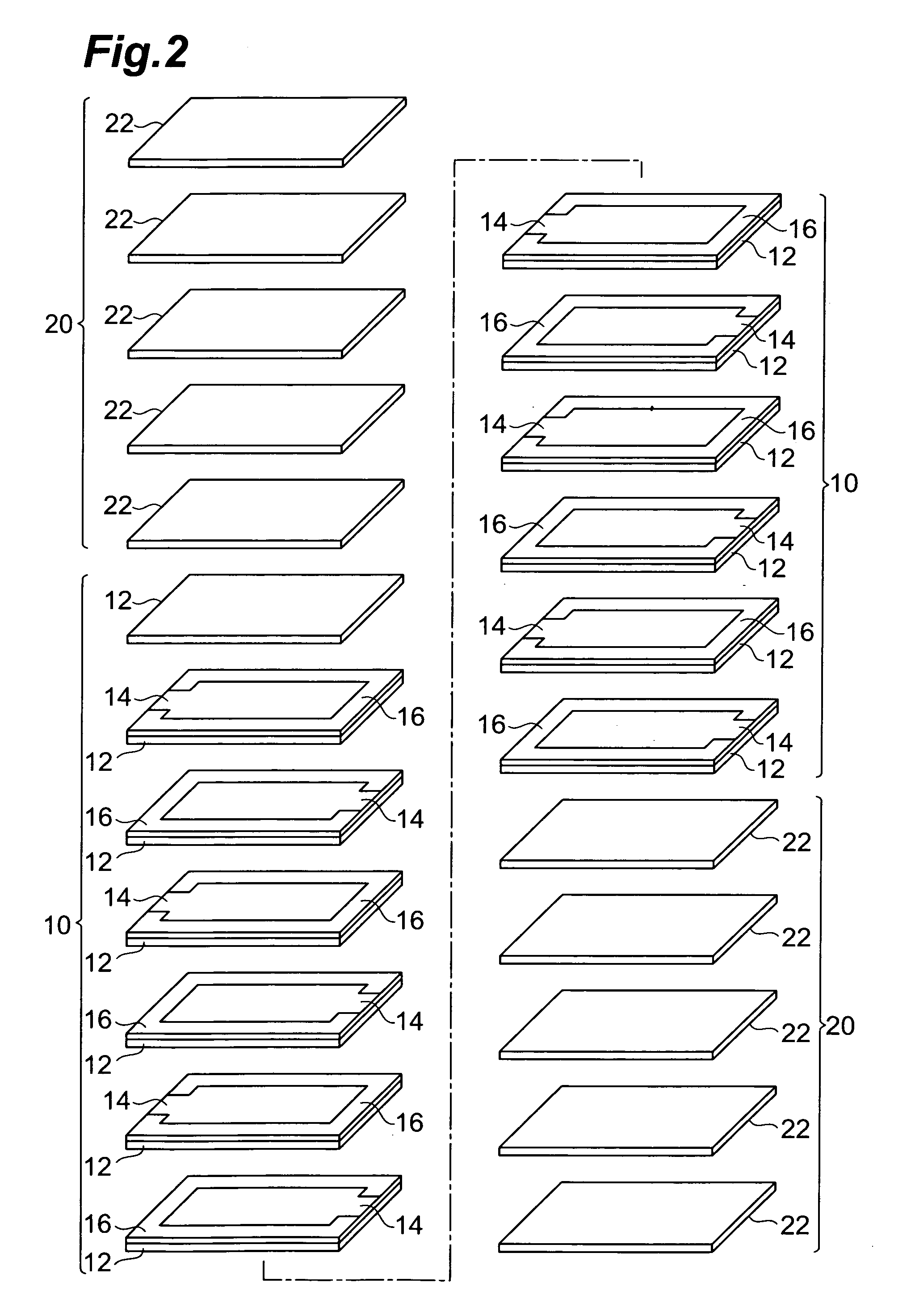
[0026] A configuration of multilayer ceramic capacitor C1 according to an embodiment will be described on the basis of FIGS. 1 and 2. FIG. 1 is a sectional view of multilayer ceramic capacitor C1 according to the embodiment. The multilayer ceramic capacitor C1, as shown in FIG. 1, comprises an inner multilayer portion 10, and a pair of outer multilayer portions 20 located so as to interpose the inner multilayer portion 10 between them. Preferably, terminal electrodes 30 are formed on outer surfaces of the multilayer ceramic capacitor C1. When the multilayer ceramic capacitor C1 is, for example, of the “1005” type, the longitudinal length is 1.0 mm, the width 0.5 mm, and the height 0.5 mm.

[0027]FI...


PUM

PropertyMeasurementUnit
thicknessaaaaaaaaaa
heightaaaaaaaaaa
widthaaaaaaaaaa

Abstract

A multilayer electronic component comprises an inner multilayer portion and a pair of outer multilayer portions. The inner multilayer portion includes a plurality of first ceramic layers and a plurality of internal circuit element conductors which are alternately laminated and contain a glass component. A component amount ratio of an amount of the glass component in the second ceramic layers to an amount of a principal component of the second ceramic layers is larger than a component amount ratio of an amount of the glass component in the first ceramic layers to an amount of a principal component of the first ceramic layers.

Description

BACKGROUND OF THE INVENTION [0001] 1. Field of the Invention [0002] The present invention relates to a multilayer electronic component and a multilayer ceramic capacitor. [0003] 2. Related Background Art [0004] An example of the known multilayer electronic components of this type is one comprising a multilayer body in which a plurality of internal circuit element conductors and ceramic layers are laminated (e.g., reference is made to Patent Document 1 and Patent Document 2). The multilayer electronic component (multilayer ceramic capacitor) described in Patent Document 1 consists of an inner multilayer portion in which the internal circuit element conductors (internal electrodes) and ceramic layers are alternately laminated, and outer multilayer portions in which ceramic layers are laminated. In the multilayer electronic component (multilayer ceramic electronic component) described in Patent Document 2, the ceramic layers contain an oxide glass. [Patent Document 1] Japanese Patent ...

Claims


Application Information

Patent Timeline
Patent Type & Authority Applications(United States)
IPC IPC(8): H01G4/20H01G4/06
CPCH01G4/30H01G4/129H01G4/12
Inventor IWASAKI, AKINORIKOJIMA, TATSUYATONOGAI, TORUMUROSAWA, SHOGOMASAOKA, RAITAROABE, KYOTAROYAMAGUCHI, AKIRA
Owner TDK CORPARATION
Why Eureka
Try Eureka