Semiconductor laser device

Inactive Publication Date: 2006-12-21
PANASONIC CORP
View PDF5 Cites 6 Cited by
  • Summary
  • Abstract
  • Description
  • Claims
  • Application Information

AI Technical Summary

Benefits of technology

[0042] In addition, the coupling section may contain a material having a low thermal conductivity. Consequently, the transfer of the heat generated in the control section to the mechanism section can be prevented more effectively. Thus, it is possible to suppress the rise in the temperature of the semiconductor laser.
[0043] Moreover, it is also possible for the semiconductor laser device to further include a heat insulating section disposed between the first frame and the second frame and formed with a material having a low thermal conductivity. The transfer of the heat generated in the control section to the mechanism section can be prevented more effectively. Therefore, it is possible to suppress the rise in the temperature of the semiconductor laser.
[0044] Furthermore, a gap may be present between at least one of the heat insulating section and the first frame and the heat insulating section and the second frame, and the gap may be configured to circulate air. Consequently, the radiation of the frame can be promoted to a great extent so that the rise in the temperature of the semiconductor laser can be suppressed.
[0045] In addition, the first frame may have a first portion coming in contact with air, the second frame have a second portion coming in contact with the air, and at least one of the first portion and the second portion is provided with a concavo-convex po

Problems solved by technology

On the other hand, the upper limit of an operation guarantee temperature at which the operation of the semiconductor laser is guaranteed is low, that is, between 60 and 70° C. Furthermore, even if an operating temperature for operating the semiconductor laser ranges within the operation guarantee temperature, the lifetime of the semiconductor laser tends to be shorter when the operating temperature is raised.
Therefore, the size of the frame member becomes comparatively large.
The Peltier element described in Japanese Laid-Open Patent Publication No. 2001-338460 has a comparatively large power consumption for cooling.
In addition, the cooling fan also consumes power.
When the Peltier element and the cooling fan are driven for cooling, the duration of a battery used in the camera is reduced due to the increase in power consum

Method used


Image

  • Semiconductor laser device
  • Semiconductor laser device
  • Semiconductor laser device

Examples


Example

First Embodiment

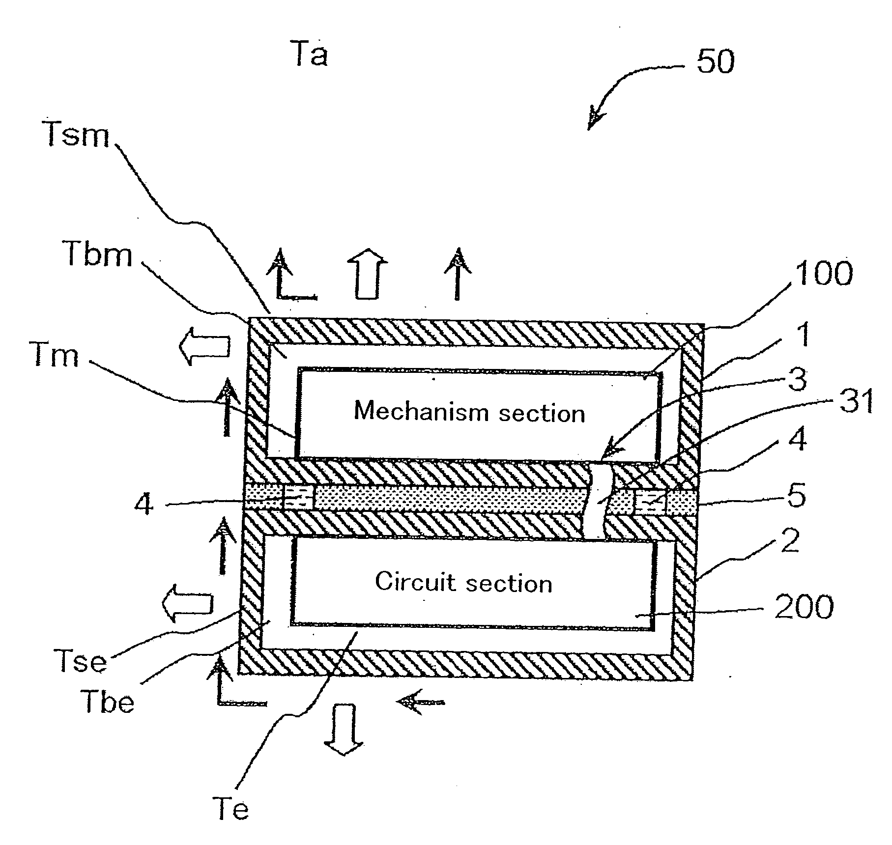
[0056]FIG. 1 is a sectional-view schematically showing an optical disk device 50 according to a first embodiment of the present invention.

[0057] The optical disk device 50 includes a mechanism section 100 including a semiconductor laser, a frame 1 for holding the mechanism section 100 and radiating heat generated in the mechanism section 100, a circuit section 200 for controlling the mechanism section 100, a frame 2 for holding the circuit section 200 and radiating heat generated in the circuit section 200, and a coupling section 4 for insulatively coupling the frame 1 to the frame 2.

[0058] The mechanism section 100 includes an optical head for performing at least one of recording and reproduction for an optical disk which is mounted. The details of the optical head will be described below with reference to FIG. 3.

[0059] The mechanism section 100 is attached to the frame 1 for the mechanism section. In the following description, the frame 1 for the mechanism sect...

Example

Second Embodiment

[0157]FIG. 4 is a sectional-view schematically showing an optical disk device 50A according to a second embodiment of the present invention.

[0158] In the optical disk device 50A, the same members as those in the optical disk device 50 described with reference to FIG. 1 in the first embodiment have the same reference numerals and their description will be omitted.

[0159] Moreover, alphabets are attached to the last of the reference numerals for the members having configurations changed in order to make a distinction.

[0160] The optical disk device 50A is different from the optical disk device 50 described with reference to FIG. 1 in the following two respects. Similarly, a frame 1 for a mechanism section will be referred to as a frame 1 and a frame 2A for a circuit section will be referred to as a frame 2A.

[0161] A first difference is that the frame 2A is provided with a hole 2Aa capable of performing ventilation. The inner part of the frame 2A is ventilated throu...

Example

Third Embodiment

[0166]FIG. 5 is a sectional-view schematically showing an optical disk device 50B according to a third embodiment of the present invention.

[0167] In the optical disk device 50B, particularly, it is assumed that a frame can be designed comparatively freely so as to be connected to USB or IEEE 1394 as peripheral equipment of personal computer (PC). As a matter of course, it is also possible to apply the optical disk device 50B to an optical disk video camera.

[0168] In the optical disk device 50B, the same members as those of the optical disk device 50 described in the first embodiment and the optical disk device 50A described in the second embodiment have the same reference numerals and the description of the members will be omitted.

[0169] Moreover, alphabetical letters are attached to the last of the reference numerals for the members having configurations changed in order to make a distinction.

[0170] The optical disk device 50B is greatly different from the opti...


PUM


Abstract

A semiconductor laser device according to the present invention includes a mechanism section having a semiconductor laser, a first frame for holding the mechanism section and radiating heat generated in the mechanism section, a control section for controlling the mechanism section, a second frame for holding the control section and radiating heat generated in the control section, and a coupling section for insulatively coupling the first frame to the second frame.

Description

TECHNICAL FIELD [0001] The present invention relates to a semiconductor laser device and more particularly to a semiconductor laser device in which a frame for radiating heat generated in a mechanism section including a semiconductor laser and a frame for radiating heat generated in a control section for controlling the mechanism section are insulatively coupled to each other. BACKGROUND ART [0002] In recent years, a technique has been developed for achieving higher data storage density in a phase transition type optical disk, using a blue semiconductor laser and utilizing an objective lens having a high NA of 0.85. [0003] When using the aforementioned technique, even if the diameter of the optical disk is small, for example approximately 5 cm, the capacity of the optical disk is 3 to 4 GB so that an optical disk having a large capacity can be implemented. [0004] By applying a compressing technique such as MPEG2 to the optical disk, it is possible to implement a genuine optical disk...

Claims


Application Information

Patent Timeline
IPC IPC(8): G11B7/00G11B33/14H01S5/024
CPCH01S5/024G11B33/1406G11B33/14H01S3/04
Inventor ISHIBASHI, KENZOGOTOH, KATSUMIYUKIMASA, TAKATOSHIICHINOSE, MAKOTO
Owner PANASONIC CORP
Why Eureka
Try Eureka