Laser assisted material deposition

a technology of laser assisted material and deposition, which is applied in the direction of chemical vapor deposition coating, basic electric elements, coatings, etc., can solve the problems of difficult thermal control, place limitations on the fabrication process, and inefficient conventional heating methods for a wide variety of gases

Inactive Publication Date: 2006-12-28
MICRON TECH INC
View PDF45 Cites 15 Cited by
  • Summary
  • Abstract
  • Description
  • Claims
  • Application Information

AI Technical Summary

Problems solved by technology

These heating processes may place limitations on the fabrication process.
For instance, reactant gases that can provide the desired resultant composition upon chemical reaction may be eliminated from being used because the chemistries of these gases may be sensitive to heating, making thermal control difficult.
In other instances, conventional heating methods may be inefficient for a wide variety of gases.
As these gases are heated, a significant percentage by mass volume may decompose into unwanted gas compositions prior to undergoing the intended chemical reaction with other materials or gases.
Then, only the non-decomposed portion of the volume of reactant gas contributes to the fabrication process, limiting the reaction efficiency.
Thus, control of the thermal characteristics for forming various materials to be used in electronic devices and systems provides a significant challenge for fabrication processes.

Method used


Image

  • Laser assisted material deposition
  • Laser assisted material deposition
  • Laser assisted material deposition

Examples


Embodiment Construction

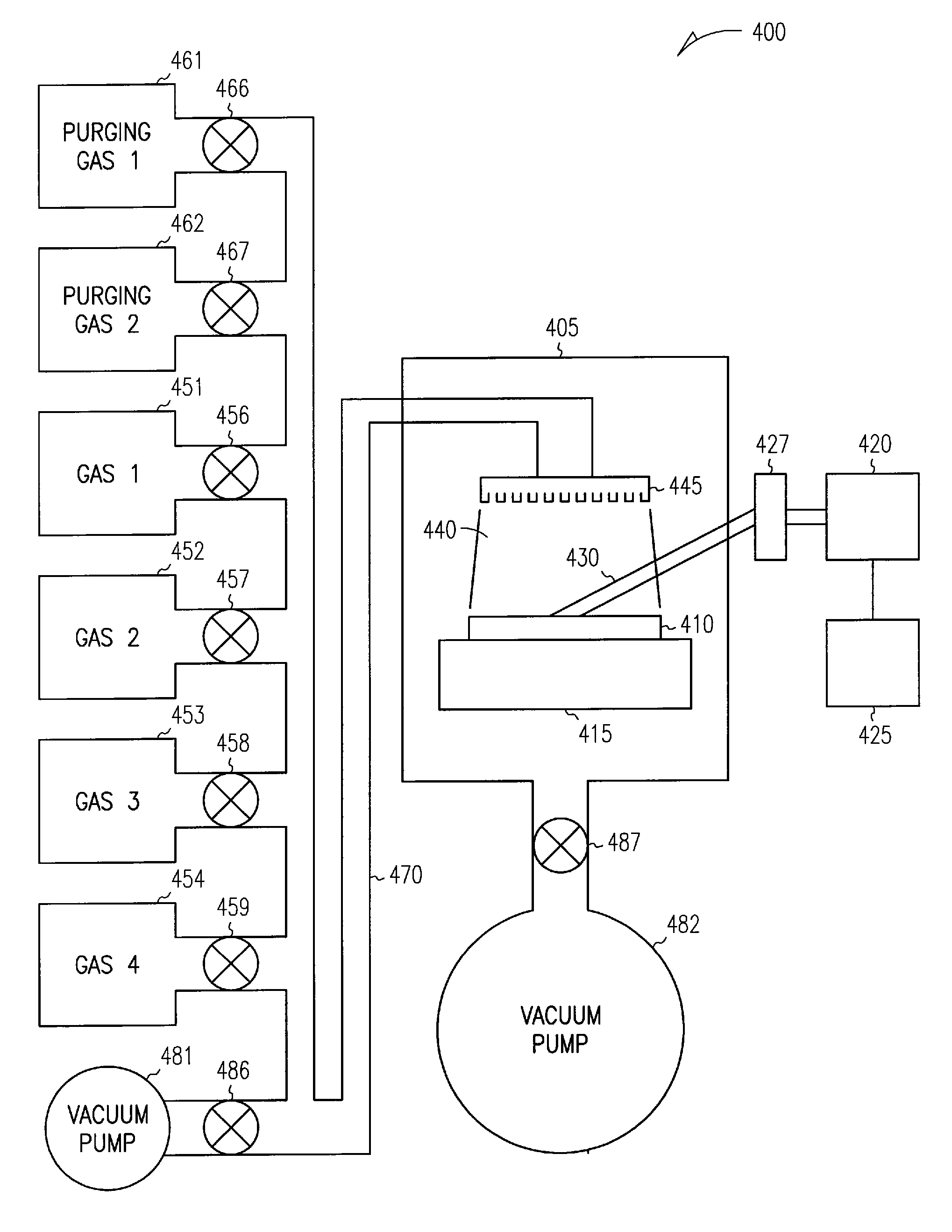
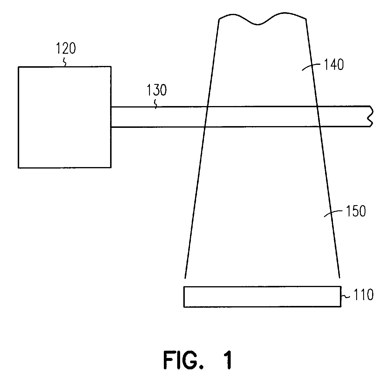
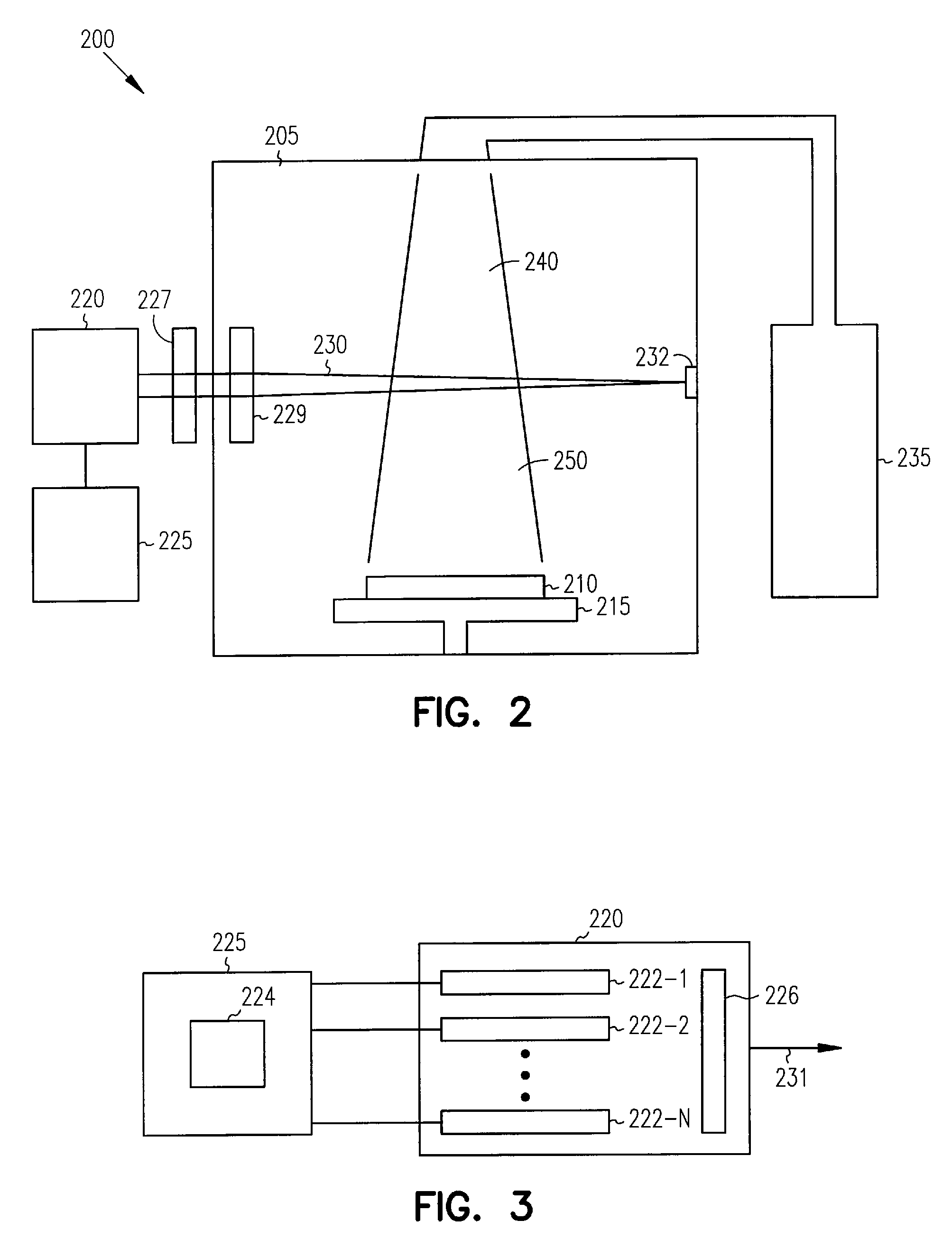
[0014] The following detailed description refers to the accompanying drawings that show, by way of illustration, specific aspects and embodiments in which the present invention may be practiced. These embodiments are described in sufficient detail to enable those skilled in the art to practice the present invention. Other embodiments may be utilized and structural, logical, and electrical changes may be made without departing from the scope of the present invention. The various embodiments disclosed herein are not necessarily mutually exclusive, as some disclosed embodiments can be combined with one or more other disclosed embodiments to form new embodiments.

[0015] The terms wafer and substrate used in the following description include any structure having an exposed surface with which to form a material composition for an integrated circuit (IC) and other electronic devices and systems. The term substrate is understood to include semiconductor wafers. The term substrate is also us...


PUM

PropertyMeasurementUnit
compositionaaaaaaaaaa
absorption frequencyaaaaaaaaaa
semiconductoraaaaaaaaaa

Abstract

Electronic devices and systems are provided with material structured from irradiation of a gas precursor with electromagnetic energy at a frequency tuned to an absorption frequency of the gas precursor. The frequency of the electromagnetic energy may be selected to impart specific amounts of energy to a gas precursor at a specific frequency that provides point of use activation of the gas precursor.

Description

RELATED APPLICATIONS [0001] This application is a Divisional of U.S. application Ser. No. 10 / 683,806, filed Oct. 10, 2003, which is incorporated herein by reference.FIELD OF THE INVENTION [0002] The present invention relates to electronic device fabrication, in particular, semiconductor device fabrication. BACKGROUND OF THE INVENTION [0003] Fabrication of electronic devices such as integrated circuits is performed through a series of processes, where each process has its own thermal characteristics. Some processes require high temperatures, while others not requiring high temperatures are performed at temperatures elevated over ambient. The elevated temperatures, whether small or large, provide an energic environment in which reactants, or precursors, interact chemically to form a desired material composition. This material composition may be an intermediate composition or the final composition forming an integral portion of the electronic device or system being constructed. [0004] ...

Claims


Application Information

Patent Timeline
Patent Type & Authority Applications(United States)
IPC IPC(8): H01L23/58C23C16/48H01L21/314H01L29/78
CPCC23C16/45523H01L29/78H01L21/3141C23C16/483H01L21/02271H01L21/0228
Inventor DANDO, ROSS S.GEALY, DANCARPENTER, CRAIG M.CAMPBELL, PHILIP H.MARDIAN, ALLEN P.
Owner MICRON TECH INC
Why Eureka
Try Eureka