Supercharge Your Innovation With Domain-Expert AI Agents!

Image display device

a display device and image technology, applied in the direction of discharge tube main electrodes, discharge tube luminescnet screens, discharge tube with screens, etc., can solve the problems of damage or degradation of electron emitter elements and thin-film electrodes, and the inability to increase the gap between the front substrate and the back substrate excessively, so as to improve display performance and reliability, and high discharge damage suppression performance

Inactive Publication Date: 2006-12-28
KK TOSHIBA
View PDF9 Cites 0 Cited by
  • Summary
  • Abstract
  • Description
  • Claims
  • Application Information

AI Technical Summary

Benefits of technology

The present invention aims to provide an image display device that can suppress discharge damage and improve display performance and reliability. The device includes a front substrate with a phosphor screen and a metal back layer, and a back substrate with electron emitter elements. The metal back layer has divisional electrodes composed of at least two row segments and column segments that connect end portions of the row segments. This design helps to reduce the likelihood of discharge damage and improve display performance and reliability.

Problems solved by technology

However, the gap between the front substrate and back substrate cannot excessively be increased, from the standpoint of characteristics of resolution and spacers.
Thus, in the FED, it is inevitable that an intense electric field is produced in a small gap between the front substrate and back substrate, and discharge between both substrates becomes a problem.
If no measure is taken to suppress discharge damage, a discharge occurs and causes damage or degradation to the electron emitter elements and thin-film electrodes connected thereto, as well as to the phosphor surface, driver ICs, driving circuits, etc.
It is very difficult to realize this, however.
By these prior-art techniques, however, it is difficult to sufficiently suppress discharge damage to the image display surface and electron emitter elements.
With the technique of Patent Document 3 wherein a coating of an electrically conductive material is provided to suppress a surface creeping discharge between the divided parts, it is not expectable to obtain a sufficient performance because of restrictions to materials.
To form an additional layer is not desirable from the standpoint of cost, mass-productivity and damage to the metal back.

Method used


Image

  • Image display device
  • Image display device
  • Image display device

Examples


Embodiment Construction

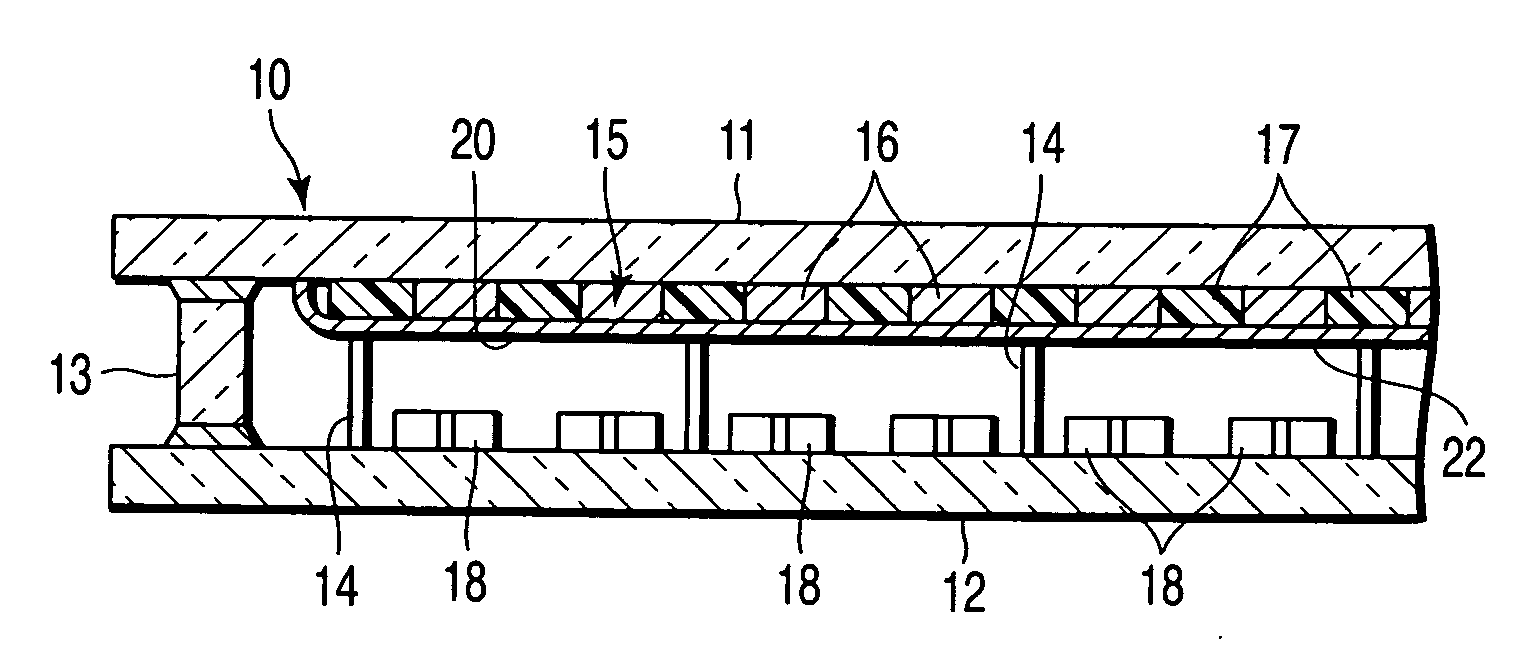
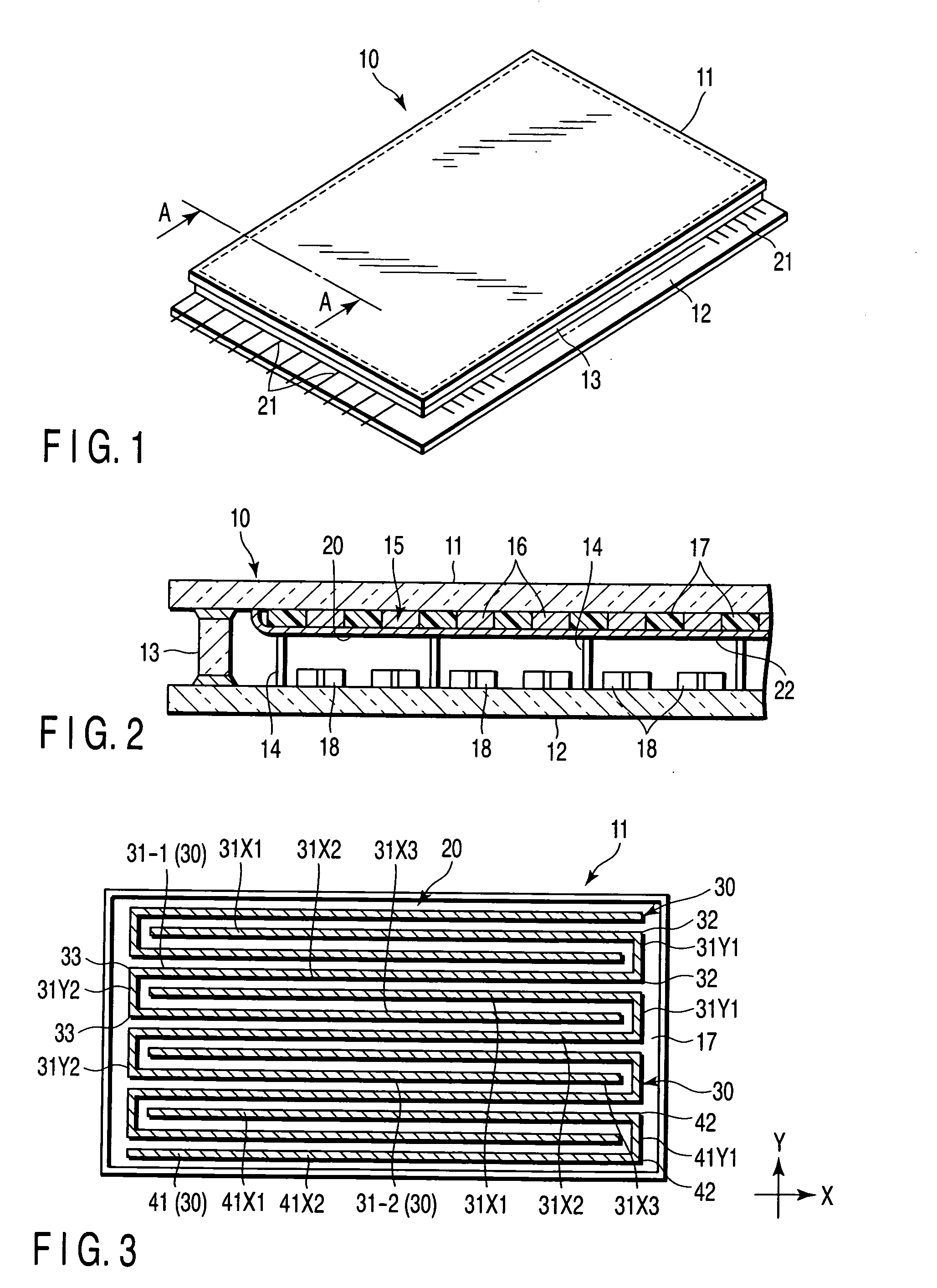
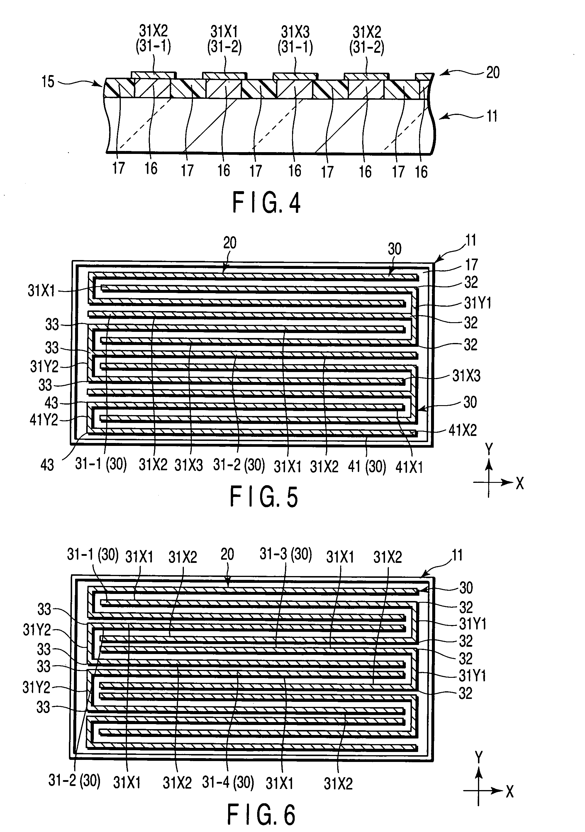
[0023] An image display device according to an embodiment of the present invention will now be described with reference to the accompanying drawings. An FED having surface-conduction electron emitter elements is described as an example of the image display device.

[0024] As is shown in FIG. 1 and FIG. 2, the FED includes a front substrate 11 and a back substrate 12, which are disposed to be opposed to each other with a gap of 1 to 2 mm. Each of the front substrate 11 and back substrate 12 is formed of a rectangular glass plate with a thickness of 1 to 3 mm. Peripheral edge parts of the front substrate 11 and back substrate 12 are attached via a rectangular-frame-shaped side wall 13, thereby forming a flat, rectangular vacuum envelope 10 in which a high-level vacuum of 10−4 Pa or less is maintained.

[0025] A plurality of spacers 14, which support an atmospheric pressure load acting on the front substrate 11 and back substrate 12, are provided within the vacuum envelope 10. The spacer...


PUM


Abstract

A front substrate, which is included in an image display device, has a metal back layer which is laid over a phosphor screen and is composed of a plurality of insular divisional electrodes. The divisional electrode is composed of at least two row segments extending in a row direction X, and column segments which extend in a column direction Y and connect end portions of the row segments.

Description

CROSS-REFERENCE TO RELATED APPLICATIONS [0001] This is a Continuation Application of PCT Application No. PCT / JP2005 / 005930, filed Mar. 29, 2005, which was published under PCT Article 21(2) in Japanese. [0002] This application is based upon and claims the benefit of priority from prior Japanese Patent Application No. 2004-110118, filed Apr. 2, 2004, the entire contents of which are incorporated herein by reference. BACKGROUND OF THE INVENTION [0003] 1. Field of the Invention [0004] The present invention relates to an image display device, and more particularly to a discharge damage suppression technique for an image display device using electron emitter elements. [0005] 2. Description of the Related Art [0006] In recent years, a flat-screen image display device, in which a great number of electron emitter elements are arranged and disposed to be opposed to an image display surface, has been developed as a next-generation image display device. There are various types of electron emitt...

Claims


Application Information

Patent Timeline
Patent Type & Authority Applications(United States)
IPC IPC(8): H01J63/04H01J31/12H01J29/08H01J29/28
CPCH01J29/085H01J1/30H01J29/28H01J31/12
Inventor TSUNEMI, MASATAKAMURATA, HIROTAKAIBUKI, HIROAKIHARAGUCHI, YUUJI
Owner KK TOSHIBA
Features
  • R&D
  • Intellectual Property
  • Life Sciences
  • Materials
  • Tech Scout
  • Unparalleled Data Quality
  • Higher Quality Content
  • 60% Fewer Hallucinations
Learn More