CMOS transistor and method of manufacturing the same

a technology of cmos transistor and metal oxide, which is applied in the direction of semiconductor devices, semiconductor/solid-state device details, electrical devices, etc., can solve the problems of affecting the performance of the channel region of the nmos transistor, and achieve the effect of simplifying the manufacturing process and improving the performance properties

Active Publication Date: 2006-12-28
SAMSUNG ELECTRONICS CO LTD
View PDF9 Cites 58 Cited by
  • Summary
  • Abstract
  • Description
  • Claims
  • Application Information

AI Technical Summary

Benefits of technology

[0009] Embodiments of the invention provide a Complementary Metal Oxide Semiconductor (CMOS) transistor having improve performance properties for both first and second conductivity type transistors, and such improvement comes by way of a simplified manufacturing process.

Problems solved by technology

Thus, application of one remedy intended to improve the performance of the channel region in a PMOS transistor may actually impair the performance of the channel region in the NMOS transistor, and vice verses.

Method used


Image

  • CMOS transistor and method of manufacturing the same
  • CMOS transistor and method of manufacturing the same
  • CMOS transistor and method of manufacturing the same

Examples


Embodiment Construction

[0017] Advantages and features of the present invention and methods of accomplishing the same will be understood by reference to the following description of embodiments with reference to the accompanying drawings. It should be noted, however, that the invention may be embodied in many different forms and should not be construed as being limited to only the embodiments set forth herein. Rather, these embodiments are provided as teaching example. Throughout the specification and drawings, like reference numerals refer to like or similar elements.

[0018] A exemplary Complementary Metal Oxide Semiconductor (CMOS) transistor and a related method of manufacture according to embodiments of the invention will now be described with reference to FIGS. 1 through 11.

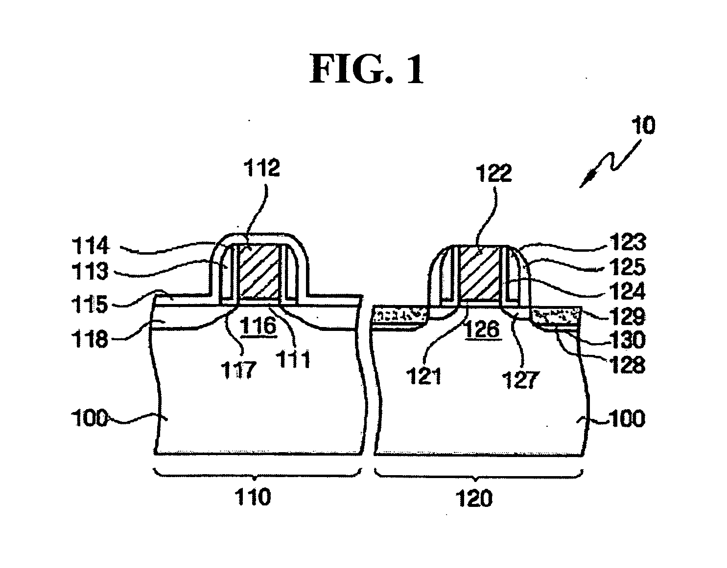
[0019]FIG. 1 is a cross-sectional view of a Complementary Metal Oxide Semiconductor (CMOS) transistor according to an embodiment of the present invention. Referring to FIG. 1, a CMOS transistor 10 includes a first conductivity typ...


PUM


Abstract

A CMOS transistor structure and related method of manufacture are disclosed in which a first conductivity type MOS transistor comprises an enhancer and a second conductivity type MOS transistor comprises a second spacer formed of the same material as the enhancer. The second conductivity type MOS transistor also comprises a source/drain region formed in relation to an epitaxial layer formed in a recess region.

Description

BACKGROUND OF THE INVENTION [0001] 1. Field of the Invention [0002] Embodiments of the invention relate to a Complementary Metal Oxide Semiconductor (CMOS) transistor and a related method of manufacture. More particularly, embodiments of the invention relate to a CMOS transistor formed from a simplified manufacturing process yielding simultaneous improvements in the performance properties of first and second conductivity type MOS transistors, and a related method of manufacture. [0003] This application claims priority to Korean Patent Application No. 10-2005-0016722 filed on Feb. 28, 2005, the subject matter of which is hereby incorporated by reference. [0004] 2. Description of the Related Art [0005] As semiconductor devices have become more highly integrated, the length of the gate in constituent MOS transistor has been progressively reduced. As the gate length in MOS transistors has been reduced, the effective length of the corresponding channel region for the MOS transistors has ...

Claims


Application Information

Patent Timeline
Patent Type & Authority Applications(United States)
IPC IPC(8): H01L21/8238H01L29/80
CPCH01L21/823807H01L21/823814H01L21/823842H01L29/7848H01L29/6656H01L29/6659H01L29/66636H01L21/823864H01L27/092
Inventor LEE, YOUNG-EUNLEE, SEONG-GHILSHIN, YU-GYUNLEE, JONG-WOOKKIM, YOUNG-PIL
Owner SAMSUNG ELECTRONICS CO LTD
Why Eureka
Try Eureka