Preventing damage to metal using clustered processing and at least partially sacrificial encapsulation

Active Publication Date: 2006-12-28
TWITTER INC
View PDF13 Cites 13 Cited by
  • Summary
  • Abstract
  • Description
  • Claims
  • Application Information

AI Technical Summary

Benefits of technology

[0011] A third aspect of the invention is related to a method of forming a substantially damage-free metal in a semiconductor device, the method comprising the steps of: forming a metal in a layer of the semiconductor device; forming a structure over the metal; forming an opening in the structure exposing a metal surface in a bottom of the opening, the ope

Problems solved by technology

During processing, however, lag times in processing leave the metal exposed.
Exposure of the metal to an ambient environment, other materials used in the processing or even adjacent dielectric structure during the lag times can cause damage to the metal.
The damaged metal results in yield and reliability problems.
In addition, other situations such as unplanned tool down times and tool overload increases metal exposure time.
In either event, the resulting circuitry may exhibit increased via resistance, via opens, wire shorts, and degraded reliability (i.e., via resistance increase during use in the field or increased cu

Method used


Image

  • Preventing damage to metal using clustered processing and at least partially sacrificial encapsulation
  • Preventing damage to metal using clustered processing and at least partially sacrificial encapsulation
  • Preventing damage to metal using clustered processing and at least partially sacrificial encapsulation

Examples


Embodiment Construction

[0022] With reference to the accompanying drawings, FIG. 3 shows a schematic representation of a clustered tool 100 including at least one clustered chamber 102A-E (only five shown), including an etching chamber (e.g., 102A). Each embodiment of the invention uses clustered tool 100 such that metal is not exposed to an ambient prior to being encapsulated according to the invention. “Clustered” indicates that different chambers of the same etching tool are used and a robot handler (not shown) is used to move wafers 103 from a load lock 104 between chambers.

[0023] Turning to FIGS. 4-11, methods of preventing metal exposure to ambient during semiconductor fabrication will now be described.

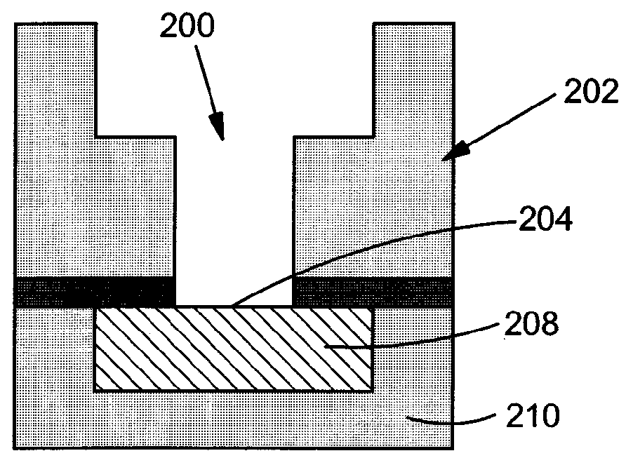
[0024] Referring to FIG. 4, in one general embodiment, a first step includes forming an opening (e.g., a dual damascene opening) 200 in a structure 202 exposing a metal surface 204 in a bottom of opening 200. Structure 202 may include any now known or later developed dielectric material such as fluor...


PUM


Abstract

Methods are disclosed for metal encapsulation for preventing exposure of metal during semiconductor processing. In one embodiment, the method includes forming an opening in a structure exposing a metal surface in a bottom of the opening, where the opening forming step occurs in a tool including at least one clustered chamber. An at least partially sacrificial encapsulation layer is then formed on the exposed metal surface in the tool to prevent reaction of the exposed metal surface with the ambient. Exposure of the metal is thereby prevented.

Description

BACKGROUND OF THE INVENTION [0001] 1. Technical Field [0002] The present invention relates generally to semiconductor fabrication, and more particularly, to methods of preventing damage of a metal during lag times in semiconductor fabrication by using clustered processing and an at least partially sacrificial encapsulation layer. [0003] 2. Related Art [0004] During semiconductor fabrication, metal that forms circuitry is formed in various materials. Metals such as copper (Cu) are typically lined with a liner material such as tantalum nitride, which prevents interaction of the metal with other materials. During processing, however, lag times in processing leave the metal exposed. Exposure of the metal to an ambient environment, other materials used in the processing or even adjacent dielectric structure during the lag times can cause damage to the metal. The damaged metal results in yield and reliability problems. Lag times can be created and or extended by a number of situations. Fo...

Claims


Application Information

Patent Timeline
IPC IPC(8): H01L21/4763
CPCH01L21/76814H01L21/76831H01L21/76834H01L21/76865H01L21/76844H01L21/76849H01L21/76843
Inventor GAMBINO, JEFFREY P.STAMPER, ANTHONY K.
Owner TWITTER INC
Why Eureka
Try Eureka