Semiconductor device

Active Publication Date: 2006-12-28
SEMICON ENERGY LAB CO LTD
View PDF13 Cites 25 Cited by
  • Summary
  • Abstract
  • Description
  • Claims
  • Application Information

AI Technical Summary

Benefits of technology

[0030] In the semiconductor device of the present invention, the second conductive layer and the third conductive layer which connects the first conductive layer and the second conductive layer are connected to each other in the contact hole and at least a part of an end portion of the third conductive layer is located inside the contact hole. In other words, near the contact hole where the second conductive layer is connected to the third conductive layer, the third conductive layer does not overlap with the second conductive layer with the first insulating layer interposed therebetween and the end portion of the third conductive layer is not formed over the first insulating layer. For this reason, it is possible to decrease depression and projection of the third conductive layer.
[0031] Thus, depression and projection of the second insulating layer formed over the third conductive layer can also be decreased. In the case of forming the second insulating layer having superior flatness by a coating method, it is not necessary to form the second insulating layer thick; therefore, the material can be reduced. This makes it possible to achieve cost reduction and high productivity.
[0032] In the case of forming the second insulating layer with a photosensitive material, it is possible to form the second insulating layer with relatively un

Problems solved by technology

In a liquid crystal display device, if an element for driving a pixel electrode is formed by using such a thin film transistor, depression and projection of the insulating layer cause an orientation film not to be rubbed uniformly.
This causes problems in that orientation of liquid crystals is distorted and accordingly image quality is degraded.
As a result, as compared with the case of forming an insulating layer over an insulating layer and wires that have little depression and pr

Method used


Image

  • Semiconductor device
  • Semiconductor device
  • Semiconductor device

Examples


embodiment mode 1

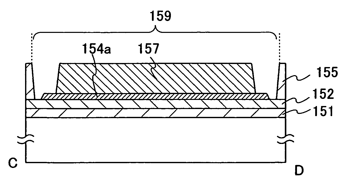
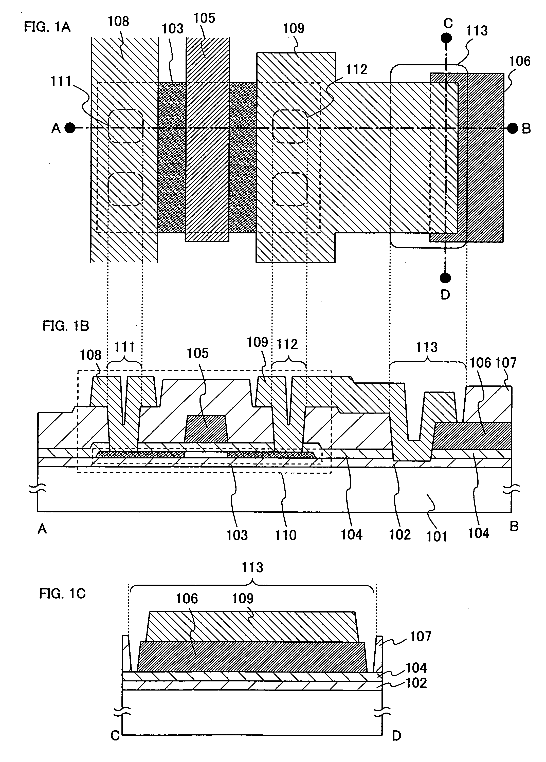
[0061] This embodiment mode will describe a semiconductor device in which a plurality of conductive layers formed with an insulating layer interposed therebetween are connected to each other inside a contact hole and at least a part of an end portion of one conductive layer is located inside the contact hole. Typically, with reference to FIGS. 1A to 1C, this embodiment mode will describe a semiconductor device which includes a third conductive layer connected to a first conductive layer and a second conductive layer, in which the second conductive layer and the third conductive layer are connected to each other inside a contact hole, in which an end portion of the third conductive layer is located inside the contact hole, and in which the third conductive layer is connected to the first conductive layer and the second conductive layer in different contact holes.

[0062] Here, one of a source region and a drain region of a semiconductor region of a first transistor is used as the firs...

embodiment mode 2

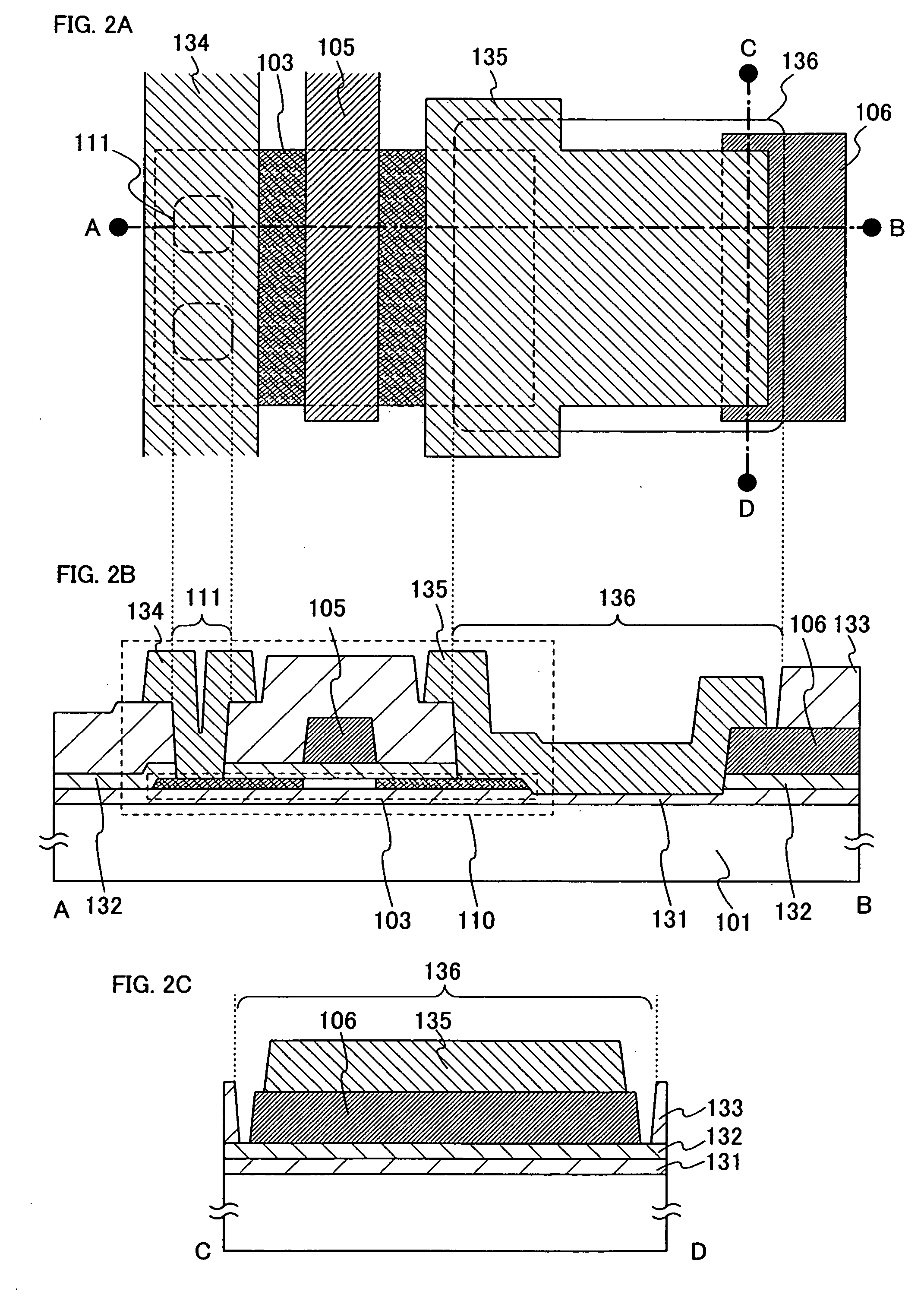
[0097] This embodiment mode will describe a semiconductor device with reference to FIGS. 2A to 2C, which has a third conductive layer connected to a first conductive layer and a second conductive layer. In this semiconductor device, the second conductive layer is connected to the third conductive layer in a contact hole, an end portion of the third conductive layer is located inside the contact hole, and the first conductive layer is connected to the third conductive layer in the same contact hole as the contact hole where the second conductive layer is connected to the third conductive layer.

[0098] Similarly to Embodiment Mode 1, one of a source region and a drain region of a semiconductor region of a first transistor is used as the first conductive layer, a gate electrode of a second transistor is used as the second conductive layer, and a wire for connecting the gate electrode and the one of the source region and the drain region is used as the third conductive layer. The first ...

embodiment mode 3

[0110] Embodiment Mode 3 will describe a semiconductor device with reference to FIGS. 3A to 3C, in which a part of the second conductive layer overlaps with a part of the first conductive layer in Embodiment Mode 2.

[0111] In this embodiment mode, similarly to Embodiment Mode 1, one of a source region and a drain region of a semiconductor region of a first transistor is used as the first conductive layer, a gate electrode of a second transistor is used as the second conductive layer, and a wire for connecting the gate electrode to the one of the source region and the drain region is used as the third conductive layer. The first transistor and the second transistor are thin film transistors.

[0112]FIG. 3A is a top view of the first transistor, and FIGS. 3B and 3C are cross-sectional views taken along lines A-B and C-D of FIG. 3A, respectively. In FIG. 3A, the substrate 101, the insulating layers 102 and 143, and the gate insulating layer 104 which are shown in FIGS. 3B and 3C are omi...


PUM


Abstract

A semiconductor device of the present invention has a first conductive layer, a second conductive layer, an insulating layer which is formed between the first conductive layer and the second conductive layer and which has a contact hole, and a third conductive layer which is connected to the first conductive layer and the second conductive layer and of which at least a part of an end portion is formed inside the contact hole. Near a contact hole where the second conductive layer is connected to the third conductive layer, the third conductive layer does not overlap with the second conductive layer with the first insulating layer interposed therebetween and an end portion of the third conductive layer is not formed over the first insulating layer. This allows suppression of depression and projection of the third conductive layer.

Description

BACKGROUND OF THE INVENTION [0001] 1. Field of Invention [0002] The present invention relates to a semiconductor device in which wires are stacked. [0003] 2. Description of the Related Art [0004] In recent years, the degree of integration of semiconductor elements increases for wiring substrates and semiconductor devices, and integration progresses further. This makes wire width narrower and increases the number of wires. Moreover, downsizing of an area of semiconductor devices is attempted by making the wiring into multi-wiring. [0005] As a typical example of a semiconductor element that forms a semiconductor device, a thin film transistor is described with reference to FIGS. 16A to 16C. FIG. 16A is a top view of a thin film transistor and FIGS. 16B and 16C are cross-sectional views taken along lines A-B and C-D of FIG. 16A, respectively. In FIG. 16A, a substrate 101, insulating layers 102, 107, and 115, and a gate insulating layer 104 which are shown in FIGS. 16B and 16C are omitt...

Claims


Application Information

Patent Timeline
IPC IPC(8): H01L21/44H01L23/48H05B44/00
CPCH01L29/42384H01L29/78621H01L2924/0002H01L27/124H01L27/1288H01L2924/00H01L27/1214
Inventor YAMAZAKI, SHUNPEISAKAKURA, MASAYUKIMIYAZAKI, AYA
Owner SEMICON ENERGY LAB CO LTD
Why Eureka
Try Eureka