Printing substrate for liquid crystal display, and manufacturing method thereof

Active Publication Date: 2007-01-04
LG DISPLAY CO LTD
View PDF7 Cites 19 Cited by
  • Summary
  • Abstract
  • Description
  • Claims
  • Application Information

AI Technical Summary

Benefits of technology

[0014] An advantage of the present invention is to provide a printing substrate for a liquid crystal display which may mitigate the shortcoming of a resist printing process to implement minute patterns and thus improve pattern resolution and transcription property.
[0015] Another advantage of the present invention is to provide a manufacturing method of a printing substrate for a liquid crystal display which may efficiently manufacture a printing substrate for the liquid crystal display.
[0016] Additional features and advantages of the invention will be set forth in the description which follows, and in part will be apparent from the description or may be learned by practice of the invention. These and other advantages of the invention will be likely realized and attained by the structure particularly pointed out in the written description and claims hereof as well as the appended drawings.
[0017] To achieve these and oth

Problems solved by technology
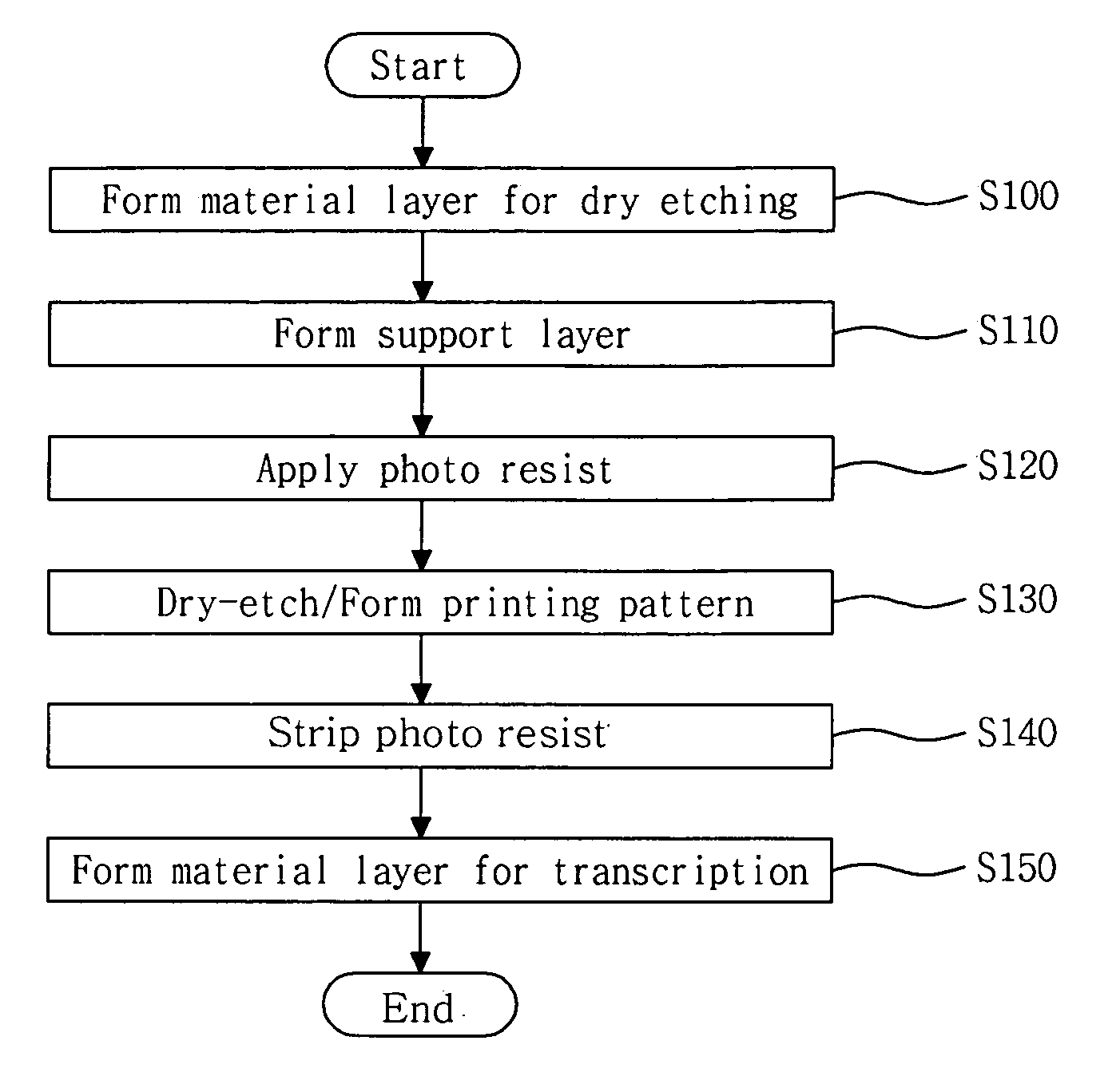
As such, since the wet etching has an isotropic etching property which shows a uniform etching property without respect to the direction of crystal faces, loss to critical dimension (CD) greatly occurs due to a collective wet etching upon forming the printing pattern P1, and thus this makes it difficult to manufacture a precise printing substrate having minute patterns formed thereon.
However, if the printing substrate is manufactured through the wet etching, loss in thickness occurs on both sides of the printing substrate by the factor of d2.
As an ex

Method used


Image

  • Printing substrate for liquid crystal display, and manufacturing method thereof
  • Printing substrate for liquid crystal display, and manufacturing method thereof
  • Printing substrate for liquid crystal display, and manufacturing method thereof

Examples


first embodiment

[0030]FIG. 8 is a view illustrating the printing substrate for the liquid crystal display according to the present invention.

[0031] In FIG. 8, the printing substrate for the liquid crystal display according to the first embodiment of the present invention comprises a transparent insulating substrate 200, and a material layer 210 for dry etching. The material layer 210 for dry etching constitutes a printing pattern on an upper surface of the transparent insulating substrate 200.

[0032] The material layer 210 for dry etching may be formed of a Si-based material, such as a-Si, SiNx, SiOx, etc., which creates little loss of critical dimension during dry etching and thus performs dry etching well and provides a good transcription property.

[0033] In terms of a-Si, the a-Si may be easily deposited through a process such as PECVD (Plasma Enhanced Chemical Vapor Deposition), with a thickness formed of about 3 μm˜30 μm.

[0034] As such, since the printing pattern formed with the material laye...

second embodiment

[0036]FIG. 9 is a view illustrating the printing substrate for the liquid crystal display according to the present invention.

[0037] Referring to FIG. 9, a printing substrate for a liquid crystal display according to the second embodiment of the present invention comprises a transparent insulating substrate 200, a material layer 210 for dry etching, and a support layer 220. The material layer 210 for dry etching is formed on an upper surface of the transparent insulating substrate 200, and the support layer 220 covers a lower surface of the transparent insulating substrate 200.

[0038] The printing substrate manufactured as the first embodiment of the present invention has a great thickness in the material layer 210 for dry etching deposited on the transparent insulating substrate 200, and this may cause bending of the transparent insulating substrate 200 due to the increase of film stress.

[0039] To prevent this, the support layer 220, which may mitigate the increased stress, is depo...

third embodiment

[0041]FIG. 10 is a view illustrating the printing substrate for the liquid crystal display according to the present invention.

[0042] In FIG. 10, a printing substrate for a liquid crystal display according to the third embodiment of the present invention comprises a transparent insulating substrate 200, a material layer 210 for dry etching, and a material layer 230 for transcription. The material layer 210 for dry etching is formed on an upper surface of the transparent insulating substrate 200 to constitute a printing pattern, and the material layer 230 for transcription covers an upper surface of the transparent insulating substrate 200 including the material layer 210 for dry etching.

[0043] The material layer 230 for transcription may be formed of a metal or metal oxide.

[0044] The printing substrate should have a selection ratio which makes the transcription property good and the photo resist (PR) attached well so as to provide a good transcription from a blanket onto the printi...


PUM

PropertyMeasurementUnit
Widthaaaaaaaaaa
Widthaaaaaaaaaa
Depthaaaaaaaaaa

Abstract

The present invention relates to the implementation of minute patterns and thus improving pattern resolution and transcription property. Provided is a printing substrate for a liquid crystal display comprising a transparent insulating substrate, and a material layer for dry etching formed on an upper surface of the transparent insulating substrate, the material layer for dry etching constituting a printing pattern, and a manufacturing method of a printing substrate for a liquid crystal display comprising forming a material layer on a transparent insulating substrate, applying a photo resist along a printing pattern on the upper side of the material layer, dry-etching the material layer along the printing pattern using the photo resist as an etching mask, and striping the photo resist.

Description

[0001] This application claims the benefit of Korean Patent Application No. 10-2005-0058871, filed on Jun. 30, 2005, which is hereby incorporated by reference for all purposes as if fully set forth herein. BACKGROUND OF THE INVENTION [0002] 1. Field of the Invention [0003] The present invention relates to a printing substrate for a liquid crystal display and a manufacturing method thereof. [0004] 2. Discussion of the Related Art [0005]FIG. 1 is a view for illustrating a related art resist printing method. [0006] In the resist printing method of FIG. 1, a photo resist pattern P2 is not directly transcribed from a first transparent insulating substrate 110, on which a printing pattern is patterned to be used as a printing substrate, onto a second transparent insulating substrate 120, an object to be printed, but instead, the photo resist pattern P2 is first transferred to a blanket 100 whose surface is made of silicon rubber and the like and which serves as a medium, and then is trans...

Claims


Application Information

Patent Timeline
IPC IPC(8): C23F1/00
CPCG02F1/1362G02F1/136
Inventor YOO, SOON SUNGKWON, OH NAMCHO, HEUNG LYUL
Owner LG DISPLAY CO LTD
Why Eureka
Try Eureka