Semiconductor device

a technology of semiconductor devices and semiconductor devices, applied in semiconductor devices, semiconductor/solid-state device details, electrical apparatus, etc., can solve the problems of reducing the possibility of a solder bump being generated, and so as to achieve no increase in the resistance of the external connection electrode terminal portion and no decrease in the reliability of the semiconductor devi

Inactive Publication Date: 2007-01-04
SOCIONEXT INC
View PDF5 Cites 33 Cited by
  • Summary
  • Abstract
  • Description
  • Claims
  • Application Information

AI Technical Summary

Benefits of technology

[0021] According to the present invention, the column-shaped conductors electrically connect the wiring layer and the external connection electrode terminal with each other. The column-shaped conductors can be located at any selected positions so as to prevent a local concentration of an electric current flowing between the wiring layer and the external connection electrode terminal, thereby preventing generation of electro-migration in the external connection electrode terminal and / or a foundation metal layer of the external connection electrode terminal. Accordingly, a void (cavity) is not formed inside a solder bump, which constitutes the external connection electrode terminal, and, thus, there is no increase in a resistance of the external connection electrode terminal portion or there is no decrease in reliability of the semiconductor device.

Problems solved by technology

Accordingly, there is a high possibility of a void (cavity) being generated in the solder bump.
Thus, the existence of the void gives bad influences to an operation speed of the semiconductor device and also results in a decrease in reliability of the semiconductor device.
This may invite an increase in a resistance of the external connection electrode terminal portion, and further a decrease in reliability of the semiconductor device.
Therefore, in the connection portion between the wiring layer and the external connection electrode terminal, it is required to acquire a connection structure, which does not have a possibility of generating a local concentration of an electric current.

Method used


Image

  • Semiconductor device
  • Semiconductor device
  • Semiconductor device

Examples


Embodiment Construction

[0038] A description will now be given, with reference to the drawings, of an embodiment of the present invention.

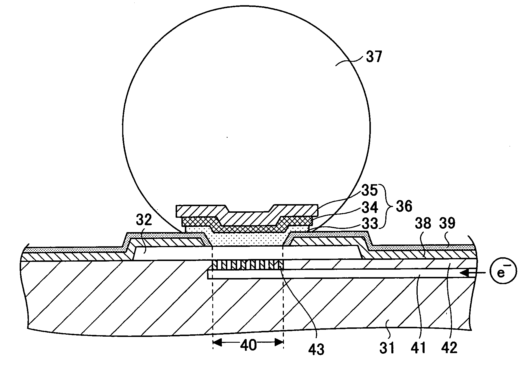
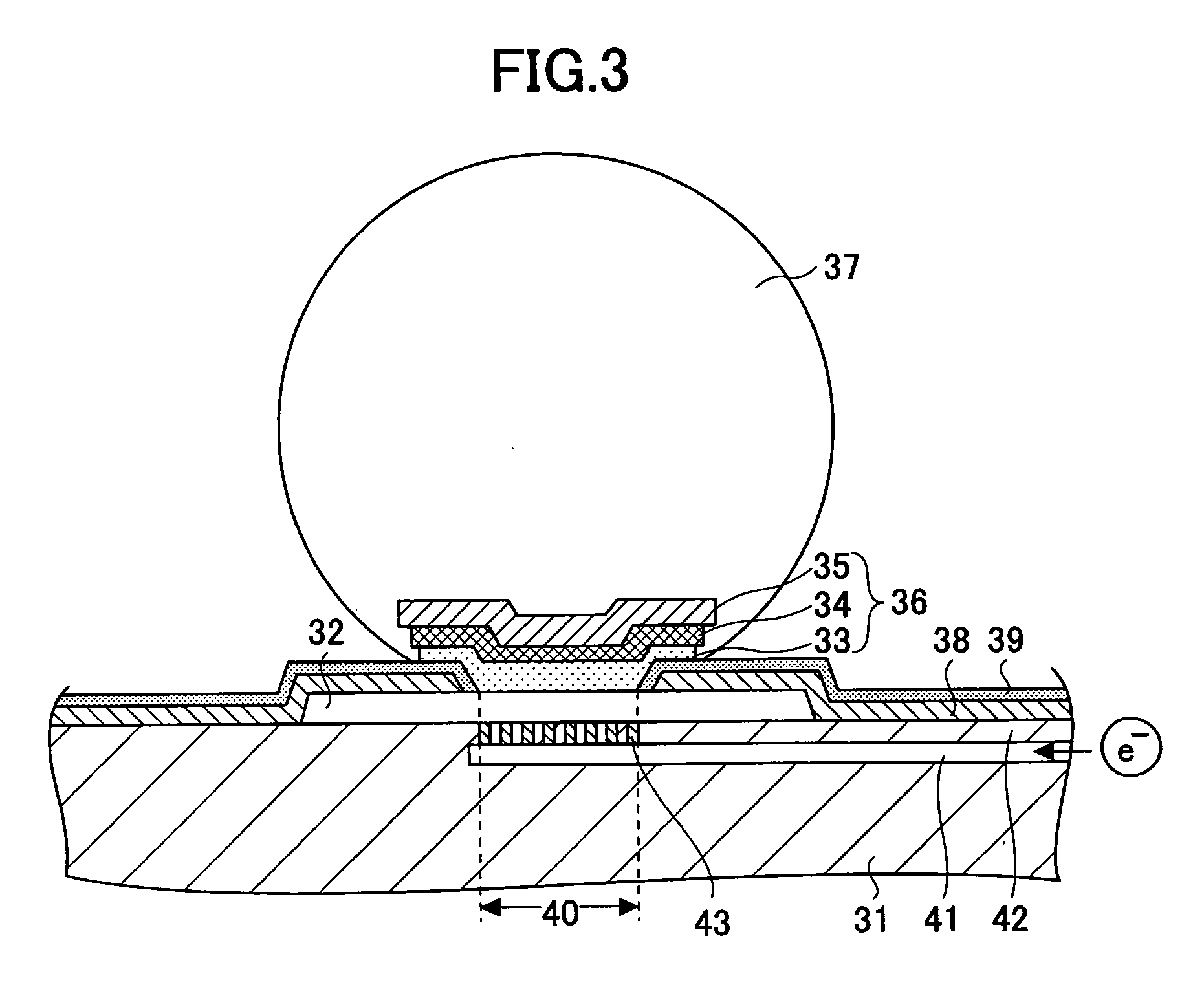
[0039]FIG. 3 shows a structure of a solder bump portion of a semiconductor device according to the embodiment of the present invention, the semiconductor device having an external connection electrode terminal formed by a solder bump as a wiring structure of the semiconductor device.

[0040] In FIG. 3, a terminal pad portion 32 is formed in an aluminum (Al) wiring layer formed on one of main surfaces of a semiconductor substrate 31. A solder bump 37 formed of a tin (Sn)-silver (Ag) solder is provided on the terminal pad portion 32 via a foundation metal layer 36 constituted by a titanium (Ti) layer 33, a copper (Cu) layer 34 and a nickel (Ni) layer 35.

[0041] An area where the terminal pad portion 32 and the foundation metal layer 36 are in contact with each other is defined by a surface protective film containing a passivation layer 38 formed of silicon nitride and a po...


PUM


Abstract

A wiring layer is provided on a semiconductor substrate and extends in a predetermined direction. An external connection electrode terminal is provided on the wiring layer through a plurality of column-shaped conductors. The column-shaped conductors are located under the external connection electrode terminal. A density of arrangement of the column-shaped conductors is varied according to a direction of extension of the wiring layer.

Description

BACKGROUND OF THE INVENTION [0001] 1. Field of the Invention [0002] The present invention relates to a semiconductor device and, more particularly, to a connection structure of an external connection electrode terminal portion of a semiconductor element. [0003] 2. Description of the Related Art [0004] In order to achieve miniaturization, high-performance and low-cost for electronic equipments, there is a demand for miniaturization, higher-performance and low-cost in semiconductor devices to be mounted on the electronic equipments. As one of external connection electrode terminal structures of such a semiconductor device, there is a structured using a solder bump. Thus, with such a demand for miniaturization of the semiconductor devices, a solder bump as an external connection electrode terminal has also been miniaturized and reduced in a diameter. [0005] On the other hand, an amount of electric current flowing in such a semiconductor device tends to be increased so as to achieve a h...

Claims


Application Information

Patent Timeline
Patent Type & Authority Applications(United States)
IPC IPC(8): H01L21/44H01L23/48
CPCH01L23/49816H01L2924/014H01L24/12H01L2224/13099H01L2924/01002H01L2924/01013H01L2924/01022H01L2924/01029H01L2924/01033H01L2924/01047H01L2924/01074H01L2924/01082H01L2924/3025H01L2924/01005H01L2924/01006H01L24/11H01L24/05H01L24/13H01L2224/05001H01L2224/05011H01L2224/05022H01L2224/05027H01L2224/05096H01L2224/05124H01L2224/05147H01L2224/05166H01L2224/05184H01L2224/05572H01L2224/05655H01L2224/13006H01L2924/00014
Inventor MATSUOKA, YOSHIHIROIMAMURA, KAZUYUKIOSHIMA, MASAOSUZUKI, TAKASHISAWADA, TOYOJI
Owner SOCIONEXT INC
Why Eureka
Try Eureka