Method of manufacturing piezoelectric wafers of saw identification tags

a piezoelectric wafer and identification tag technology, applied in the field of identification tags, can solve the problems of large and expensive antennas, inconvenient manufacturing, and inability to encode data on saw identification tags, etc., and achieve the effect of dramatically increasing the amount of data that can be encoded on each saw identification tag

Inactive Publication Date: 2007-01-04
RF SAW COMPONENTS INC
View PDF6 Cites 9 Cited by
  • Summary
  • Abstract
  • Description
  • Claims
  • Application Information

AI Technical Summary

Benefits of technology

[0013] The present invention, therefore, introduces the broad concept of manufacturing piezoelectric wafers of SAW identification tags that employ both phase and pulse position modulation whereby the amount of data that can be encoded on each SAW identification tag is dramatically increased. Such increased data capacity allows tags to contain, e.g., globally unique numbers, which feature permits SAW identification tags to be used for identifying and tracking an unprecedented number of objects uniquely and reliably.

Problems solved by technology

The difference in cost and performance between the two types is so radical that the two categories rarely compete with one another for a particular type of use.
This combination of features also leads to certain integrated circuit (IC) cost and / or design compromises to accommodate both digital and radio frequency circuitry on a single IC.
The impact of these design compromises can be partially compensated for by use of low radio frequency (RF) operating frequencies that, in turn, lead to rather large and expensive antennas.
The most daunting problem with chip tags is the need for DC power for the chip circuitry.
The combination of environmental issues coupled with severe constraints on cost, size and weight usually requires that the tag not have a battery or other on-board power source.
It also requires added components which will either add to the cost of the microchip or to the cost of the tag for the required extra electrical components in the tag, which will also result in an increased tag size.
The most important limitation of passive powered chip tags, however, is the severe restriction on the read range of the tag because a signal that is sufficiently strong to power the tag only extends a short distance from the tag reader antenna.
The disadvantages of chipless tags include that they are range limited (several centimeters at the most) and only contain limited amounts of information.
The severity of these problems has prevented their market acceptance in spite of their low cost potential.
A huge gap exists in the automatic identification market between the very low cost bar codes and the higher performing RFID chip tags.

Method used


Image

  • Method of manufacturing piezoelectric wafers of saw identification tags
  • Method of manufacturing piezoelectric wafers of saw identification tags
  • Method of manufacturing piezoelectric wafers of saw identification tags

Examples


Embodiment Construction

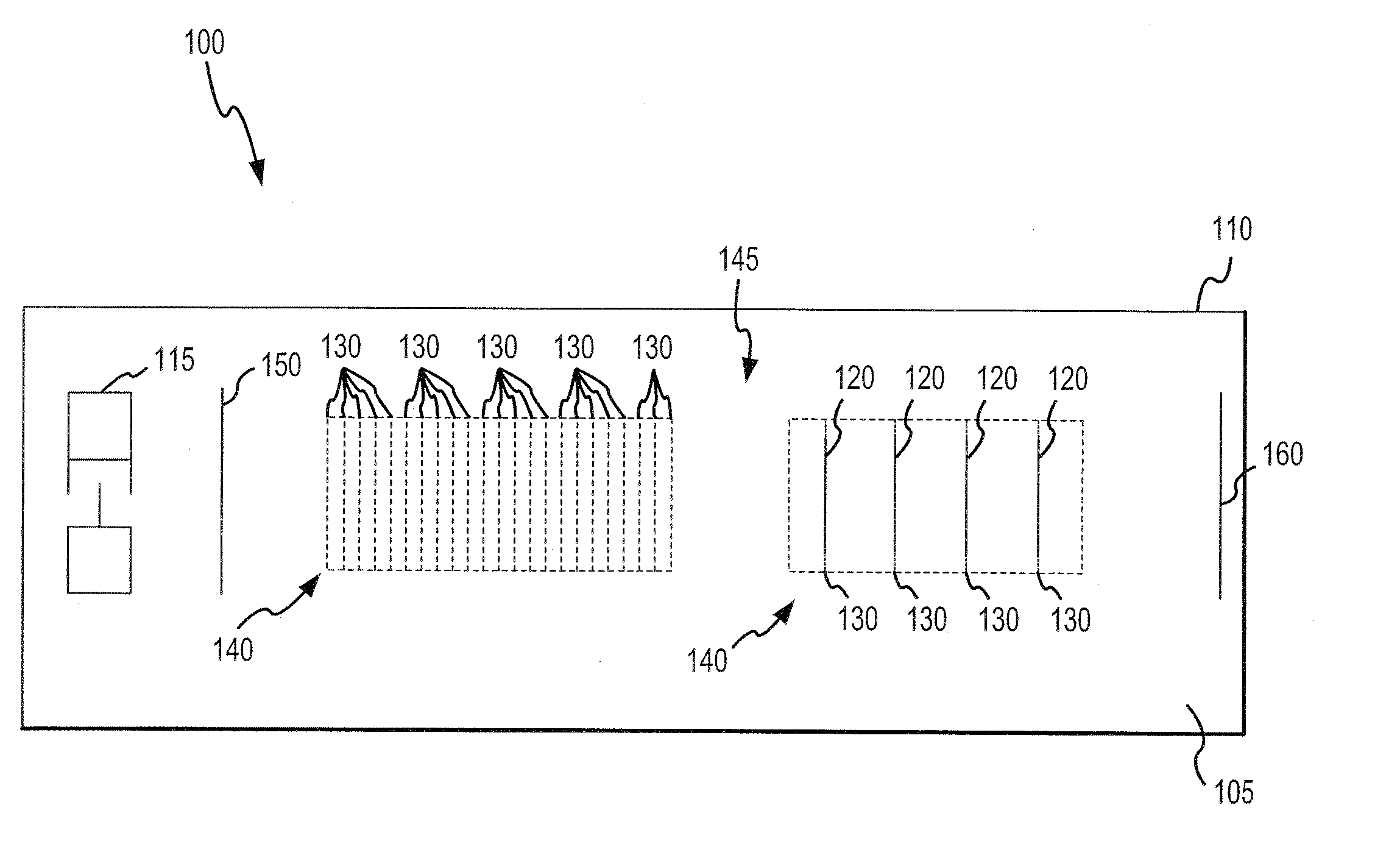
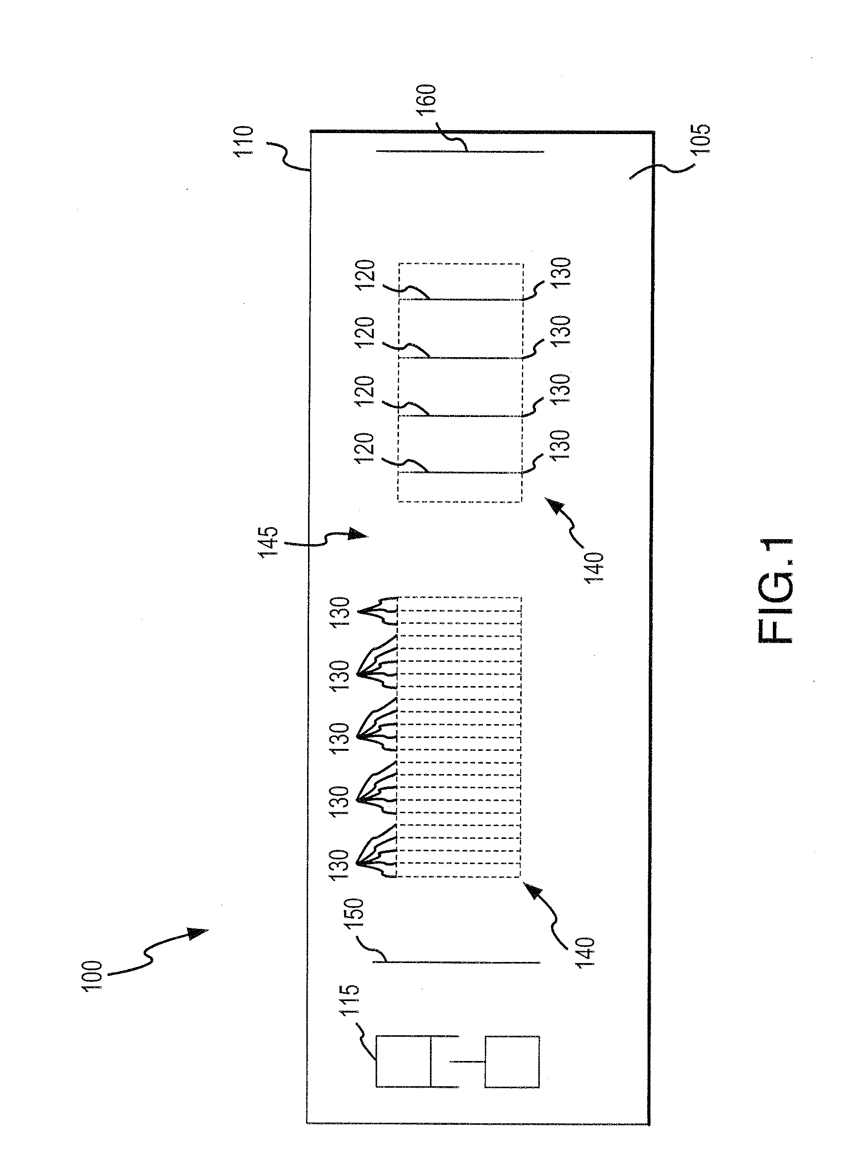
[0027] Referring initially to FIG. 1, illustrated is a plan view of a top surface 105 of a substrate 110 of an embodiment of a SAW identification tag 100 representative of those formed on piezoelectric wafers manufactured in accordance with the present invention. A description of the illustrated SAW identification tag 100 is presented to provide assistance in understanding the use of silicon or micro-electronic processing techniques to manufacture piezoelectric wafers of SAW identification tags 100. For a detailed explanation of SAW identification tags 100 of the type illustrated see U.S. patent application Ser. No. 10 / 024,624, entitled “Surface Acoustic Wave Identification Tag Having Enhanced Data Content and Methods of Operation And Manufacture Thereof,” by Hartmann, commonly assigned with the invention and incorporated herein by reference.

[0028] Located at one end of the surface 105 of the SAW identification tag 100 is a transducer 115. As those of ordinary skill in the pertinen...


PUM

PropertyMeasurementUnit
frequencyaaaaaaaaaa
frequencyaaaaaaaaaa
lengthaaaaaaaaaa

Abstract

The invention provides a method of manufacturing piezoelectric wafers of surface acoustic wave (SAW) identification tags. In one embodiment, the method includes: (1) using a master reticle to form, on each of the piezoelectric wafers, wafer-independent patterns that encode digits of a first significance for SAW identification tags; and (2) using different ones of a library of coding reticles to form, on each of the piezoelectric wafers, wafer-dependent patterns that encode digits of a second significance for SAW identification tags.

Description

CROSS-REFERENCE TO RELATED APPLICATION [0001] This application is a Divisional of prior application Ser. No. 10 / 059,700 filed on Jan. 28, 2002, currently pending to Clinton S. Hartman et al. The above-listed Application is commonly assigned with the present invention and is incorporated herein by reference as if reproduced herein in its entirety under Rule 1.53(b).TECHNICAL FIELD OF THE INVENTION [0002] The present invention is directed, in general, to a method of manufacturing identification tags and, more specifically, to a method of manufacturing a surface acoustic wave (SAW) identification tag having enhanced data content. BACKGROUND OF THE INVENTION [0003] A fascinating and increasingly important technology is that dealing with object identification systems. Such systems range from simple bar codes to very sophisticated systems still in the process of development and implementation. Among the most promising object identification systems are those using electronic tags attached ...

Claims


Application Information

Patent Timeline
Patent Type & Authority Applications(United States)
IPC IPC(8): G08B13/14G01S13/75H03H3/08H03H9/64
CPCG01S13/755G06K19/0675H03H3/08Y10T29/42Y10T29/49002Y10T29/49005Y10T29/4908H03H9/6406
Inventor HARTMANN, CLINTON S.BROWN, PAUL S.
Owner RF SAW COMPONENTS INC
Why Eureka
Try Eureka