

Method of manufacturing semiconductor device
a manufacturing method and semiconductor technology, applied in semiconductor/solid-state device manufacturing, basic electric elements, electric devices, etc., can solve the problems of large volume shrinkage, difficult silicon oxide film formation, and large volume loss
- Summary
- Abstract
- Description
- Claims
- Application Information
AI Technical Summary
Benefits of technology
Problems solved by technology
Method used
Image

Examples
first embodiment
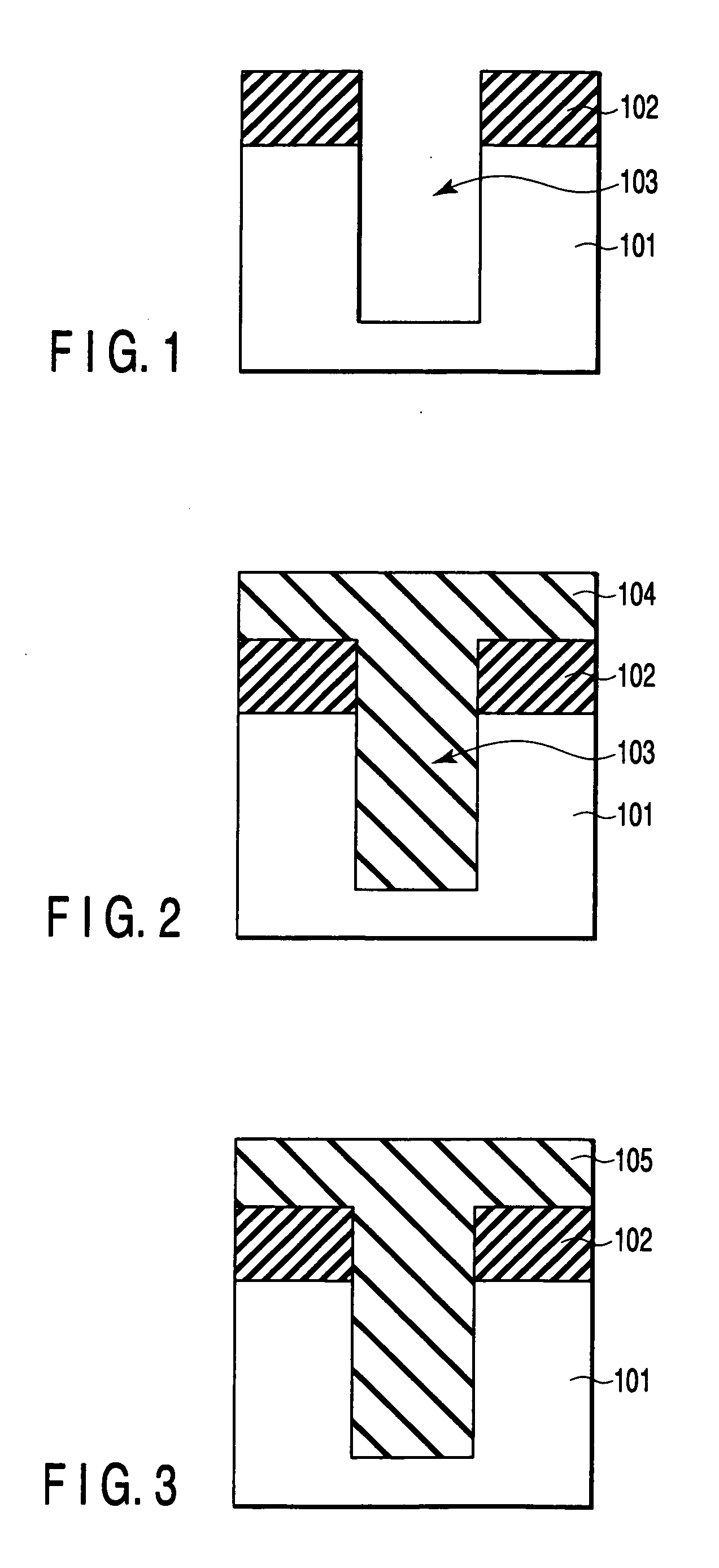
[0055] FIGS. 1 to 5 are sectional views showing a step of manufacturing a semiconductor device according to a first embodiment of the present invention.
[FIG. 1]
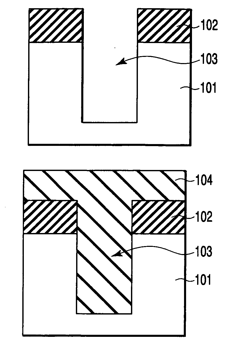
[0056] A Si3N4 film 102 is formed on a silicon substrate 101. The Si3N4 film 102 is used as a chemical mechanical polishing (CMP) stopper (polishing stopper) at the time of CMP. The thickness of the Si3N4 film 102 is, for example, about 200 nm. By using an ordinary lithography process and reactive ion etching (RIE) process, the Si3N4 film 102 and the silicon substrate 101 are processed sequentially. In this manner, a trench (isolation trench) 103 for STI is formed on a surface of the silicon substrate 101. The size of the trench 103 is, for example, about 100 nm in width and about 400 nm in depth.
[FIG. 2]
[0057] To completely fill the trench 103, a solution (perhydrogenated silazane solution) containing a perhydrosilazane polymer ((SiH2NH)n) is applied on the entire surfaces of the silicon substrate 101 and the Si3N4 film ...
second embodiment
[0084]FIG. 13 is a sectional view showing a step of manufacturing a semiconductor device according to a second embodiment of the present invention. Incidentally, in the following drawings, the parts corresponding to the already described drawings will be attached with reference numerals same as those of the already described drawings, and the detailed description thereof will be omitted.
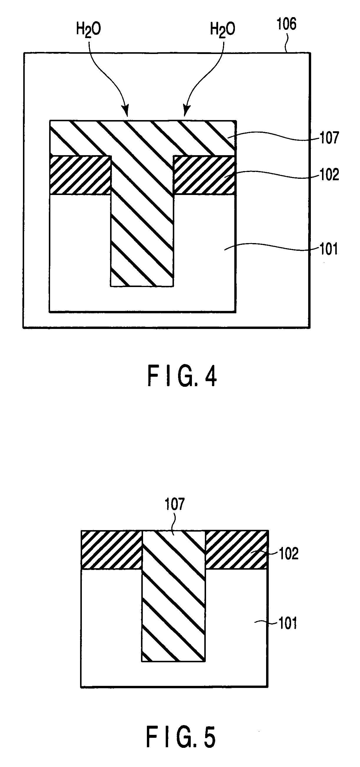
[0085] First, the steps of FIGS. 1 to 3 described in the first embodiment are performed. A SiO2 film 105 at this stage, as described above, is a SiO2 film obtained without performing sufficient oxidation to the PSZ film 104. Therefore, CMP rate of the SiO2 film 105 is insufficient.
[0086] In the first embodiment, the oxidation treatment is performed for converting the SiO2 film 105 into the SiO2 film 107 by exposing the SiO2 film 105 subjected to the first oxidation treatment in the vapor atmosphere. In the present embodiment, the oxidation treatment for converting the SiO2 film 105 into the SiO2 fi...
third embodiment
[0147] FIGS. 23 to 29 are sectional views showing a step of manufacturing a semiconductor device according to a third embodiment of the present invention. The present embodiment applies the first embodiment to a NAND type flush memory.
[FIG. 23]
[0148] A tunnel oxide film 302 is formed on a silicon substrate 301. The thickness of the tunnel oxide film 302 is about 8 nm. A polycrystalline silicon film to be processed into a floating gate electrode 303 is formed on the tunnel oxide film 302. The thickness of the polycrystalline silicon film is about 150 nm. A Si3N4 film 304 as a CMP stopper is formed on the polycrystalline silicon film. The thickness of the Si3N4 film 304 is about 100 nm.
[0149] By using an ordinary lithography process and RIE process, the Si3N4 film 304, the polycrystalline silicon film, the tunnel oxide film 302, and the silicon substrate 301 are processed sequentially, thereby, the floating gate electrode 303 is formed, and further, a trench 305 for STI is formed o...
PUM
| Property | Measurement | Unit |
|---|---|---|
| temperature | aaaaa | aaaaa |
| temperature | aaaaa | aaaaa |
| temperature | aaaaa | aaaaa |
Abstract
Description
Claims
Application Information