Recovery of hydrophobicity of low-k and ultra low-k organosilicate films used as inter metal dielectrics

a technology of organosilicate films and hydrophobicity, applied in the direction of basic electric elements, electrical apparatus, semiconductor devices, etc., can solve the problems of forming silanol, affecting the overall speed of operation of these advanced chips, and organosilicate-based materials are very sensitive to plasma exposure, etc., to achieve the effect of increasing mechanical strength and low cos

Inactive Publication Date: 2005-05-19
GLOBALFOUNDRIES INC
View PDF9 Cites 309 Cited by
  • Summary
  • Abstract
  • Description
  • Claims
  • Application Information

AI Technical Summary

Benefits of technology

[0016] It is therefore an aspect of the present invention to provide a low cost, non-disruptive method to increase the mechanical strength by altering the cage to network ratio of the porous organosilicate resin after the deposition and cure.

Problems solved by technology

With progress in the transistor device technology leading to the present ultra large scale integration, the overall speed of operation of these advanced chips is beginning to be limited by the signal propagation delay in the interconnection wires between the individual devices on the chips.
Although a tunable range of k values is possible with this set of very low k materials, there are several difficulties in integrating these materials with copper interconnects by the dual damascene process described above or by any other variation of the dual damascene process.
The chief difficulty is that the organosilicate-based materials are very sensitive to plasma exposures because of the relative ease of oxidation or cleavage of the Si-organic group linkage (for example, Si-methyl) which results in formation of silanol (Si—OH) groups in the film through a potential reaction with moisture in the ambient environment.
Silanols absorb water and hence increase the dielectric constant and the dielectric loss factor of the film significantly, thus negating the performance benefits expected from the very low k films.
They also increase the electrical leakage in the film and thus create a potentially unreliable interconnect structure.
Since reactive ion etch and plasma etch are key steps required in the formation of the dual damascene trench and via structure as described above, and in the removal of photoresists used in patterning the very low k materials, it is very difficult, if not impossible, to avoid plasma damage of this class of films during a prior art dual damascene integration.
However, it must be noted that none of these plasma chemistries completely succeed in preventing the loss of hydrophobicity of the very low k materials.
This is especially the case for porous low k materials which have a very large surface area and are easily susceptible to damage during the resist strip processes.
However, these materials do not possess the other properties required of a low k dielectric film such as a low thermal expansion and small pore sizes.
Another problem facing the successful integration of organosilicate-based porous materials is that they are very fragile mechanically due to their low elastic modulus, fracture toughness and hardness which often lead to failures in CMP, dicing and packaging operations.
Since it is imperative that a low dielectric constant be maintained, it is very difficult to decrease the void volume while maintaining the same mechanical strength.
Several methods (Padhi et al., J. Electrochem. Soc., 150 (1), G10-G14, (2003), and United States patent application publication US2004 / 0087135 A1 of Canaperi et al, assigned to the same assignee as that of the present invention) have been proposed to handle porous organosilicate materials with weak mechanical strengths but most of these methods are difficult to implement due to the fact that these methods either involve a nonstandard process flow or a nonstandard tool.
Therefore they are expensive to implement in production.
Thus far, it is not clear whether a similar reaction can be performed on fully formed films which, even after exposure to process chemistries that damage the film, have fewer silanols than the films that are in the process of forming.
However, it is clear from their results that HMDS in any medium is unable to recover, completely, the properties of the porous OSG film.
Similarly, TMCS is not completely effective at recovering the dielectric properties either.
However, in their study, they report that dimethyldichloro silane forms a monolayer on the top surface of the film and does not penetrate the bulk of the porous low k material.
Thus, unless the appropriate silylating medium as well as conditions for the silylation are used, it is difficult to recover the bulk dielectric properties of the low k material.
Additionally, the byproduct of any chlorine based silylating agent such as dimethyldichloro silane and TMCS is hydrogen chloride, which is corrosive and cannot be used in interconnect structures that contain copper.

Method used


Image

  • Recovery of hydrophobicity of low-k and ultra low-k organosilicate films used as inter metal dielectrics
  • Recovery of hydrophobicity of low-k and ultra low-k organosilicate films used as inter metal dielectrics
  • Recovery of hydrophobicity of low-k and ultra low-k organosilicate films used as inter metal dielectrics

Examples


embodiment 2

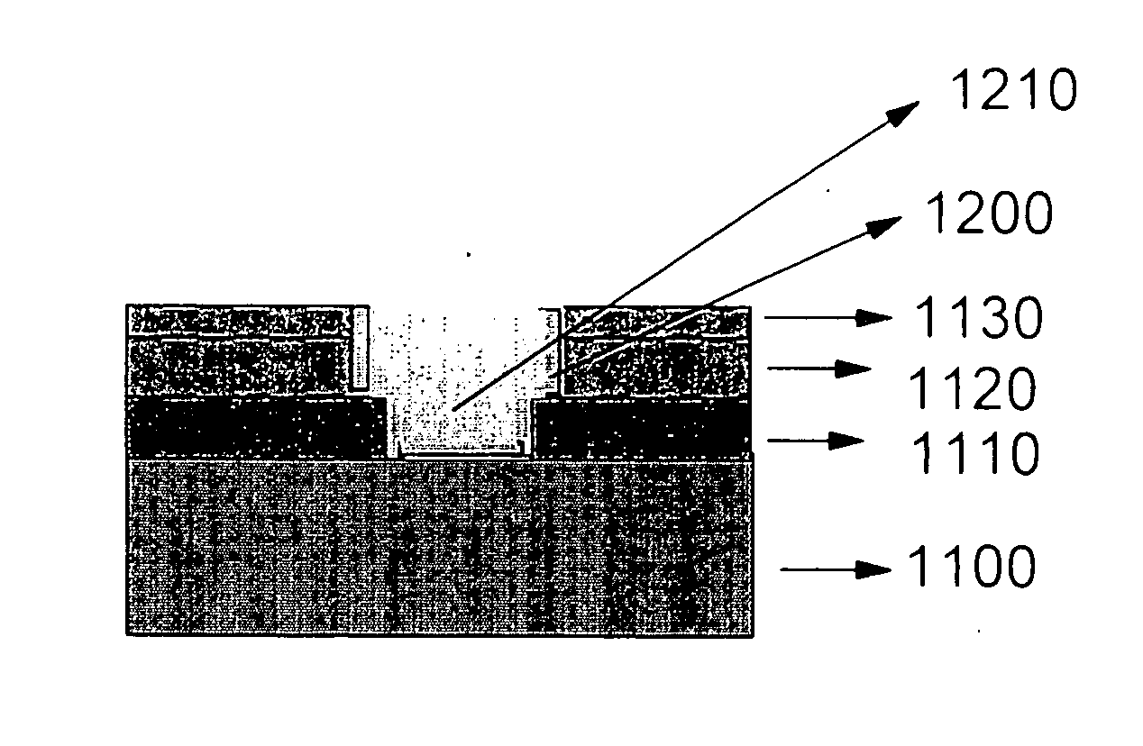
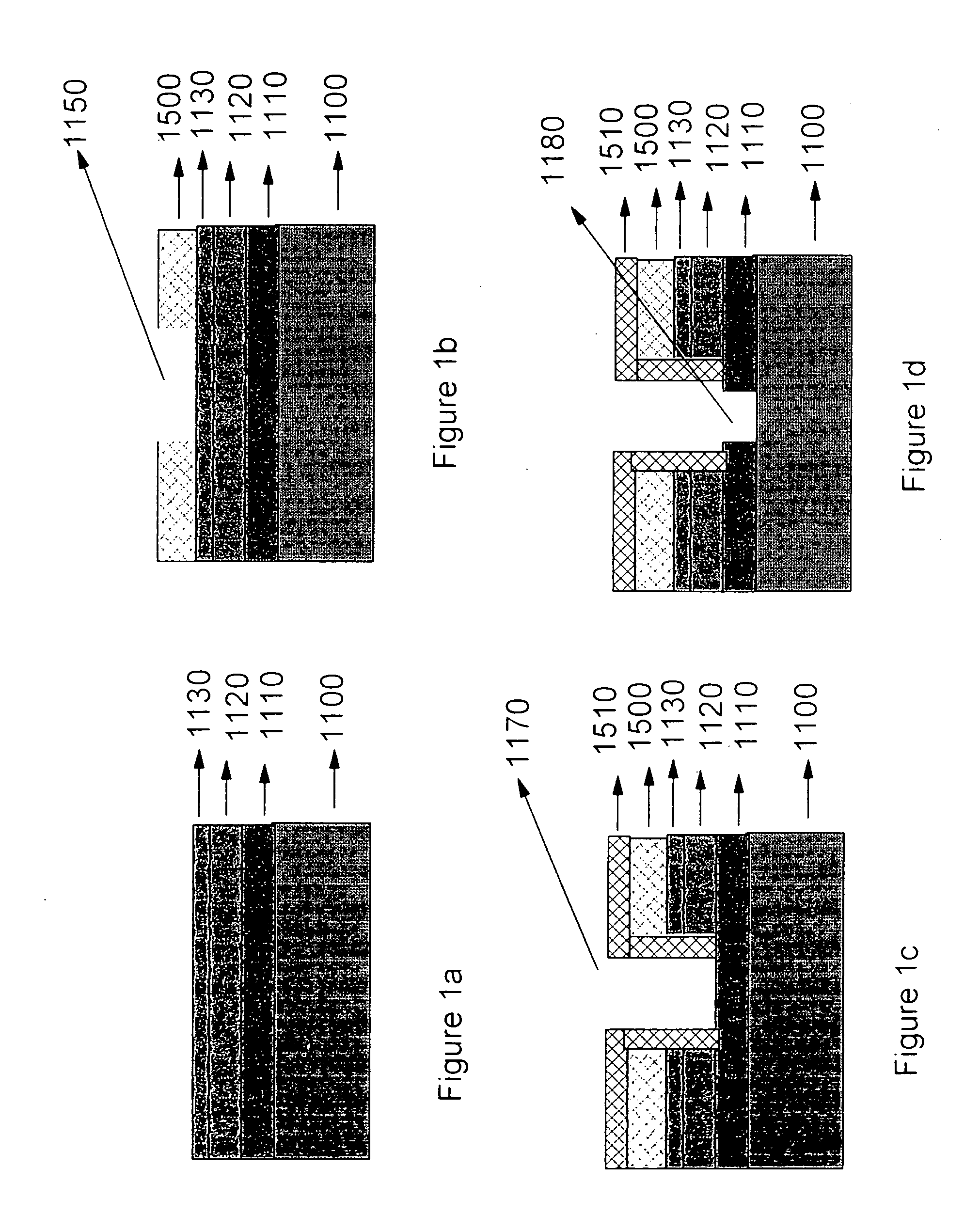
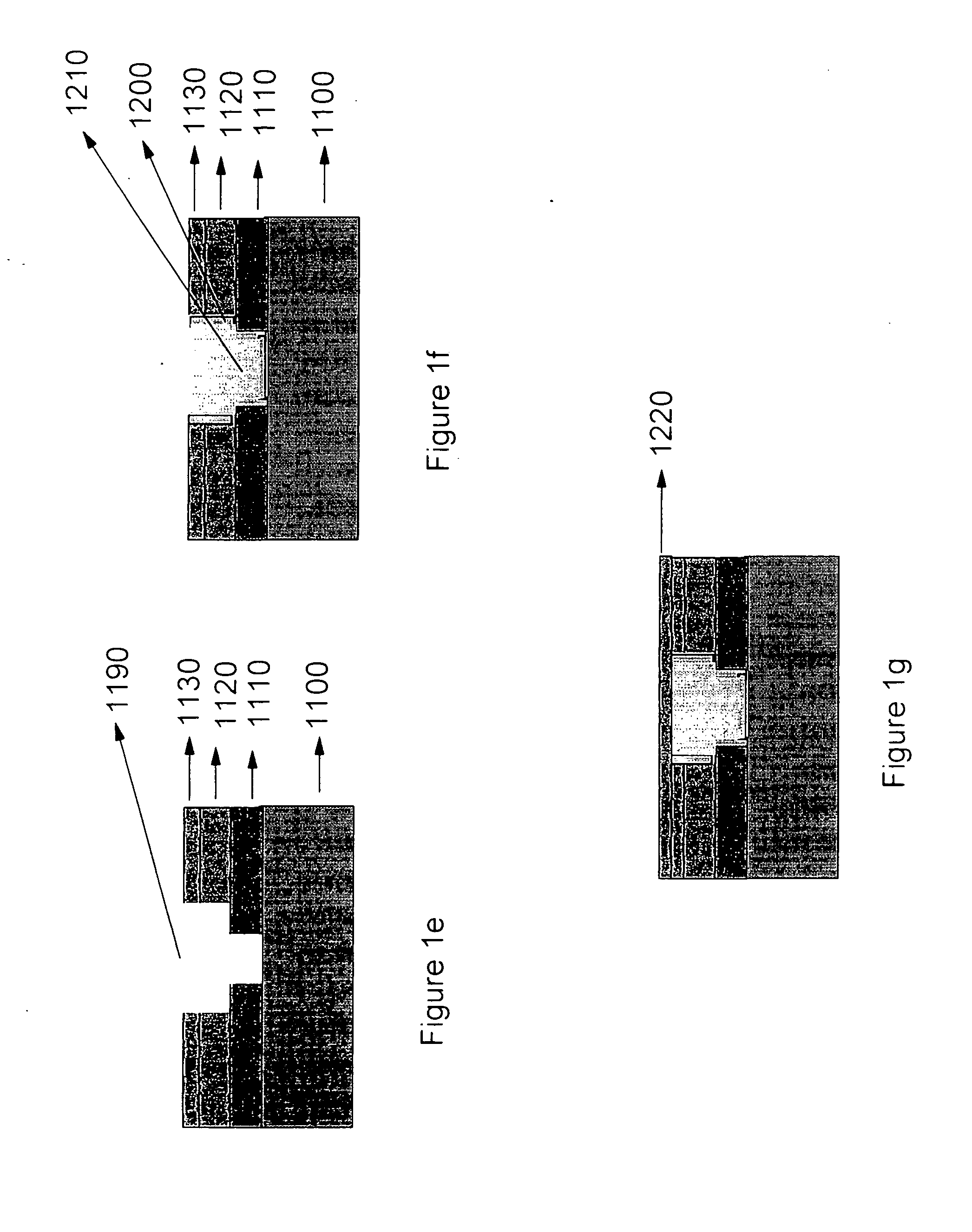
[0062] Embodiment 1 shows the efficacy of difunctional silylation agents in general and BDMADMS in particular. Embodiment 1 also shows that monofunctional silylating agents such as HMDS and TMCS are not as effective as their difunctional counterparts due to the steric hindrance presented by the three methyl moieties on the silylating agent. However, through appropriately replacing the methyl moieties on the silylating agent with the smaller hydrogen moiety, it is possible to overcome this issue. For example, in place of HMDS, the use of tetramethyldisilazane (TMDS) will result in reduced steric hindrance and a more effective silylation reaction. Similarly greater success in silylation can be demonstrated with amino, chloro and alkoxy terminated mono functional silylation agents where the methyl moieties are at least partially replaced by their hydrogen analogs. Thus, silylating agents with the general formula RXHYSi-A where X and Y are integers from 0 to 2 and 3 to 1 respectively ca...

embodiment 3

[0063] For applications where it is not necessary to penetrate the pores of the porous low k film, polymeric siloxanes with amino, alkoxy, chloro or silazanes terminated end groups with mono or di alkyl, aryl, vinyl or hydrogen moieties on them can be used to form monolayers on the top surface of the low k film and recover surface hydrophobicity. One example of such a siloxane is amino terminated polydimethylsiloxane. It is important to ensure that the molecular weight is low enough so that the silylating agent flows into the gaps created by the etch process to form trench and via in the organosilicate for the formation of the interconnect structure. As described in the embodiments above, the silylation reaction is followed by a furnace anneal to condense any remaining silanols and form new siloxane bonds that further enhance the mechanical strength.

embodiment 4

[0064] The silylating agent can also be introduced immediately after the film is deposited. The efficacy in this case depends on how many silanols are present in the film after deposition. In this embodiment, the silylation agent can also be introduced following a treatment such as UV / Ozone, or a mildly oxidizing plasma exposure that introduces silanols into the film. As in previous embodiments, the silylation is followed by a thermal anneal. Silylating agents described in any of the above three embodiments can be employed in this manner. In the case of CVD deposited films, the silylation agent can be either co-deposited or introduced into the chamber along with the precursor for the CVD dielectric.


PUM


Abstract

Often used to reduce the RC delay in integrated circuits are dielectric films of porous organosilicates which have a silica like backbone with alkyl or aryl groups (to add hydrophobicity to the materials and create free volume) attached directly to the Si atoms in the network. Si—R bonds rarely survive an exposure to plasmas or chemical treatments commonly used in processing; this is especially the case in materials with an open cell pore structure. When Si—R bonds are broken, the materials lose hydrophobicity, due to formation of hydrophilic silanols and low dielectric constant is compromised. A method by which the hydrophobicity of the materials is recovered using a novel class of silylation agents which may have the general formula (R2N)XSiR′Y where X and Y are integers from 1 to 3 and 3 to 1 respectively, and where R and R′ are selected from the group of hydrogen, alkyl, aryl, allyl and a vinyl moiety. Mechanical strength of porous organosilicates is also improved as a result of the silylation treatment.

Description

[0001] This application claims priority from Provisional Application Ser. No. 60 / 499,856 which was filed on Sep. 3, 2003.FIELD OF THE INVENTION [0002] This invention pertains to interconnect wiring networks on very high performance microelectronic chips used in computers, microprocessors, microcontrollers, sensors, communication devices and the like. In particular, the inventive structures described herein pertain to significantly reducing the signal propagation delay associated with these wires. The inventive methods detailed and claimed provide the chemistry and processing required to recover the dielectric properties of low dielectric constant dielectrics after they have been rendered hydrophilic by required plasma exposures and to the chemistry and method required to increase the mechanical strength, and maintain the low dielectric constant of porous organosilicate dielectrics after they have been deposited and during the process of building an interconnect structure comprising ...

Claims


Application Information

Patent Timeline
Patent Type & Authority Applications(United States)
IPC IPC(8): H01L21/00H01L21/3105H01L21/312H01L21/768
CPCH01L21/31058H01L21/76807H01L21/76814H01L21/76826H01L21/02203H01L2924/0002H01L21/02126H01L2924/00
Inventor CHAKRAPANI, NIRUPAMACOLBURN, MATTHEW E.DIMITRAKOPOULOS, CHRISTOS D.PFEIFFER, DIRKPURUSHOTHAMAN, SAMPATHNITTA, SATYANARAYANA V.
Owner GLOBALFOUNDRIES INC
Why Eureka
Try Eureka