Imaging array having variable conversion gain

a technology of low-light imaging and variable conversion gain, which is applied in the field of low-light imaging arrays, can solve the problems of increasing the cost of adc and the conversion time required to generate each pixel value with the number of bits, and the output voltage will be too high for conventional low-cost cmos circuitry, and the noise level of the amplifier will be too high to provide optimum performance for pixels with small charges

Active Publication Date: 2007-01-11
BAE SYST IMAGING SOLUTIONS
View PDF6 Cites 38 Cited by
  • Summary
  • Abstract
  • Description
  • Claims
  • Application Information

AI Technical Summary

Benefits of technology

[0006] The present invention includes an imaging array and a charge measurement amplifier for use in such imaging arrays. The imaging array includes a CCD imaging array having a plurality of pixels that accumulate charge when exposed to light, a readout amplifier, and a shift register. The readout amplifier includes an operational amplifier having an input and an output port and a variable feedback capacitor connecting the input and output ports. The variable feedback capacitor has a feedback capacitance determined by a gain control signal. The operational amplifier generates an output signal on the output port related to the feedback capacitance and a charge coupled to the input port. The readout amplifier also includes a reset path between the input and output ports, the path having an impedance controlled by a reset signal, and a controller. The controller generates the gain control signal and the reset signal during a charge measurement cycle. The controller generates the reset signal prior to a charge to be measured being transferred to the input port. The controller initially sets the feedback capacitance to a first capacitance value after generating the reset signal, and the controller changes the feedback capacitance from the first capacitance value to a second capacitance value during the charge measurement cycle if the output signal exceeds a first threshold value during the charge measurement cycle. The shift register sequentially shifts the charge accumulated by each pixel into the input port. The controller applies the reset signal prior to each charge being shifted into the input port. The controller generates an output signal indicative of the charge shifted into the input port and a gain signal indicative of the gain control signal at a predetermined time in the charge measurement cycle. In one embodiment, the variable feedback capacitor includes a network having a plurality of capacitors and a first gain switch, the gain switch shorting a first node within the network to the output port in response to the gain control signal having a first value. In one embodiment, each of the capacitors in the network is characterized by a capacitance value and the feedback capacitance has a value less than each of the capacitance values.

Problems solved by technology

If this conversion circuit is used to convert signals from pixels having high light intensities, the output voltages will be too high for conventional low cost CMOS circuitry.
If, on the other hand, the amplifier gain is set to a low value to maintain the signal within the range of CMOS circuitry when the charge from high intensity pixels is processed, the noise levels of the amplifier will be too high to provide optimum performance for the pixels having small charges.
Both the cost of the ADC and the conversion time required to generate each pixel value increase with the number of bits.
While additional conversion circuits or high speed ADCs can be used to compensate for this increase in readout time, both of these solutions increase the cost of the imaging array.

Method used


Image

  • Imaging array having variable conversion gain
  • Imaging array having variable conversion gain
  • Imaging array having variable conversion gain

Examples


Embodiment Construction

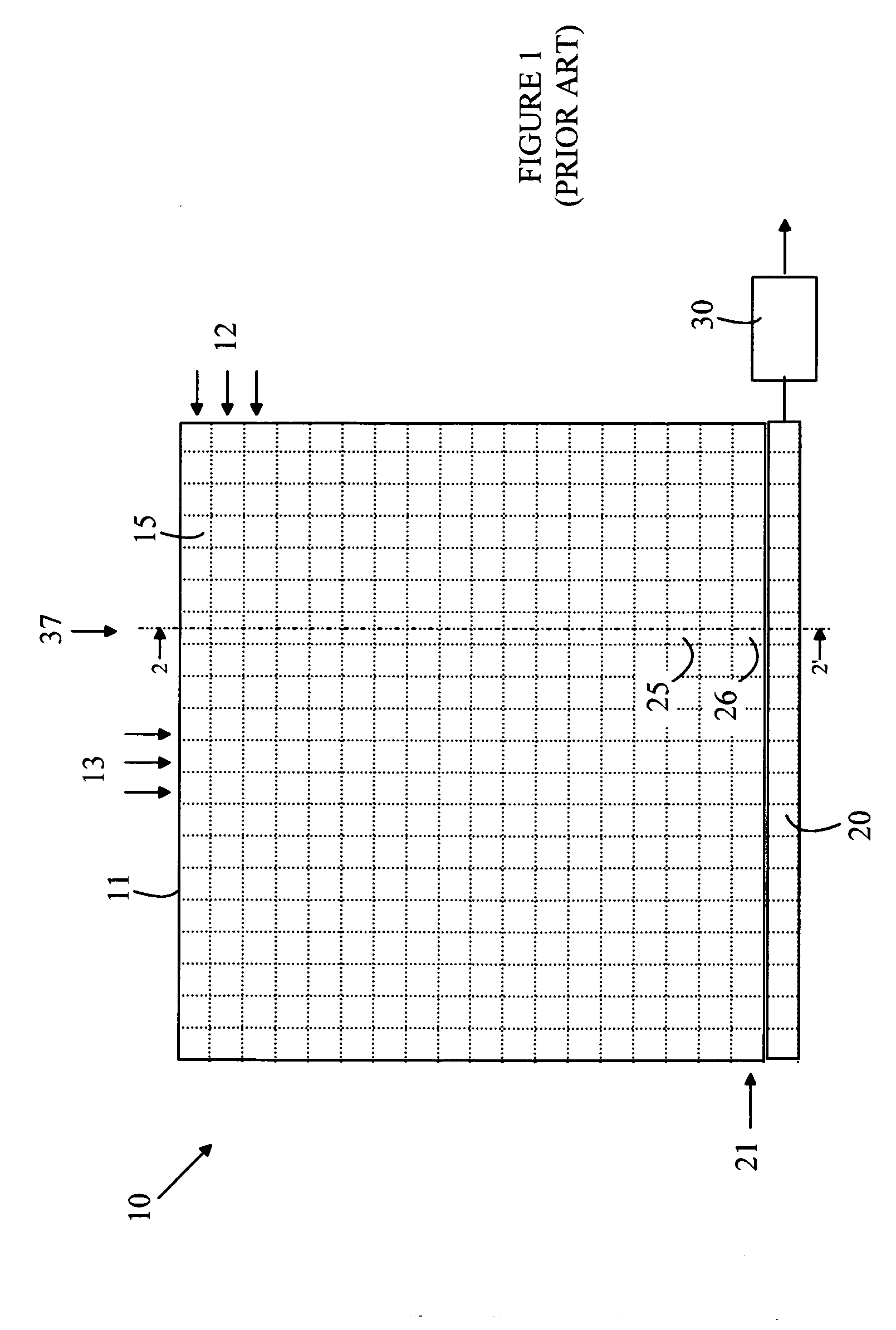
[0017] The manner in which the present invention provides its advantages can be more easily understood with reference to FIG. 1, which illustrates a CCD imaging sensor. Image sensor 10 includes a photodetector array 11 in which the individual photodetectors 15 are organized as a plurality of rows 12 and columns 13. In addition, the columns can be operated as shift registers to move charge stored in the various photodetectors after the array is exposed to an image, to a shift register 20. On each single column shift operation, the contents of the photodetectors in row 21 are shifted into register 20, and the contents of each column are moved downward toward shift register 20. The contents of shift register 20 are then shifted horizontally into an output amplifier 30 that converts the charge in cell 25 to an output voltage. To simplify the drawing, the various electrodes used in the shifting operations and the clock circuitry has been omitted from FIG. 1.

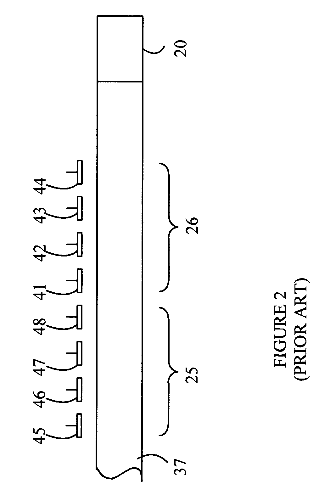
[0018] Refer now to FIG. 2, w...


PUM


Abstract

A CCD imaging array and a charge measurement amplifier for use in such imaging arrays is disclosed. The array includes a plurality of pixels that accumulate charge when exposed to light, a readout amplifier having input and output ports. The readout amplifier has a variable gain that is set by a gain control signal. The readout amplifier also includes a reset path between the input and output ports, the path having an impedance controlled by a reset signal. A controller generates the gain control signal and the reset signal during a charge measurement cycle. Initially the gain is set to a first value after generating the reset signal. The gain is changed to a second value during the charge measurement cycle if the output signal exceeds a first threshold value. The readout amplifier can be constructed from an operational amplifier having a capacitive feedback loop.

Description

BACKGROUND OF THE INVENTION [0001] The present invention may be more easily understood in the context of low light imaging arrays such as those used in digital photography to record an image. For the purposes of this discussion, an image will be defined as a two-dimensional array of digital values that represent the amount of light received during an exposure period at each pixel on a two-dimensional surface onto which the image is projected. For the purposes of this discussion, it will be assumed that each pixel is a small rectangular area on that surface. In digital photography, the image is projected onto an imaging array in which each pixel includes a photodetector that measures the amount of light that falls on some portion of the pixel area. [0002] In one class of imaging array, the detector utilizes an area of silicon to collect electrons that are generated by light that strikes the silicon. During the exposure period, the electrons accumulate in the pixel area. The charge co...

Claims


Application Information

Patent Timeline
Patent Type & Authority Applications(United States)
IPC IPC(8): H01L27/00
CPCH04N5/243H04N5/378H04N5/355H04N23/76H04N25/57H04N25/75
Inventor DO, HUNG
Owner BAE SYST IMAGING SOLUTIONS
Why Eureka
Try Eureka