Driver device and display device

a display device and drive device technology, applied in semiconductor devices, semiconductor/solid-state device details, instruments, etc., can solve the problems of inability to perform downsizing of films, substantially the same etc., to reduce the cost of film substrates, reduce the cost of products, and reduce the cost of ic chips.

Inactive Publication Date: 2007-01-11
RENESAS ELECTRONICS CORP
View PDF3 Cites 15 Cited by
  • Summary
  • Abstract
  • Description
  • Claims
  • Application Information

AI Technical Summary

Benefits of technology

[0019] Recently, the cost of the IC chip becomes substantially the same as the cost of the film. For this reason, in order to reduce the cost of the products, it is necessary to reduce the cost of the film substrate.

Problems solved by technology

Recently, the cost of the IC chip becomes substantially the same as the cost of the film.
However, the actual condition is that downsizing of the film has not been performed yet.

Method used


Image

  • Driver device and display device
  • Driver device and display device
  • Driver device and display device

Examples


Embodiment Construction

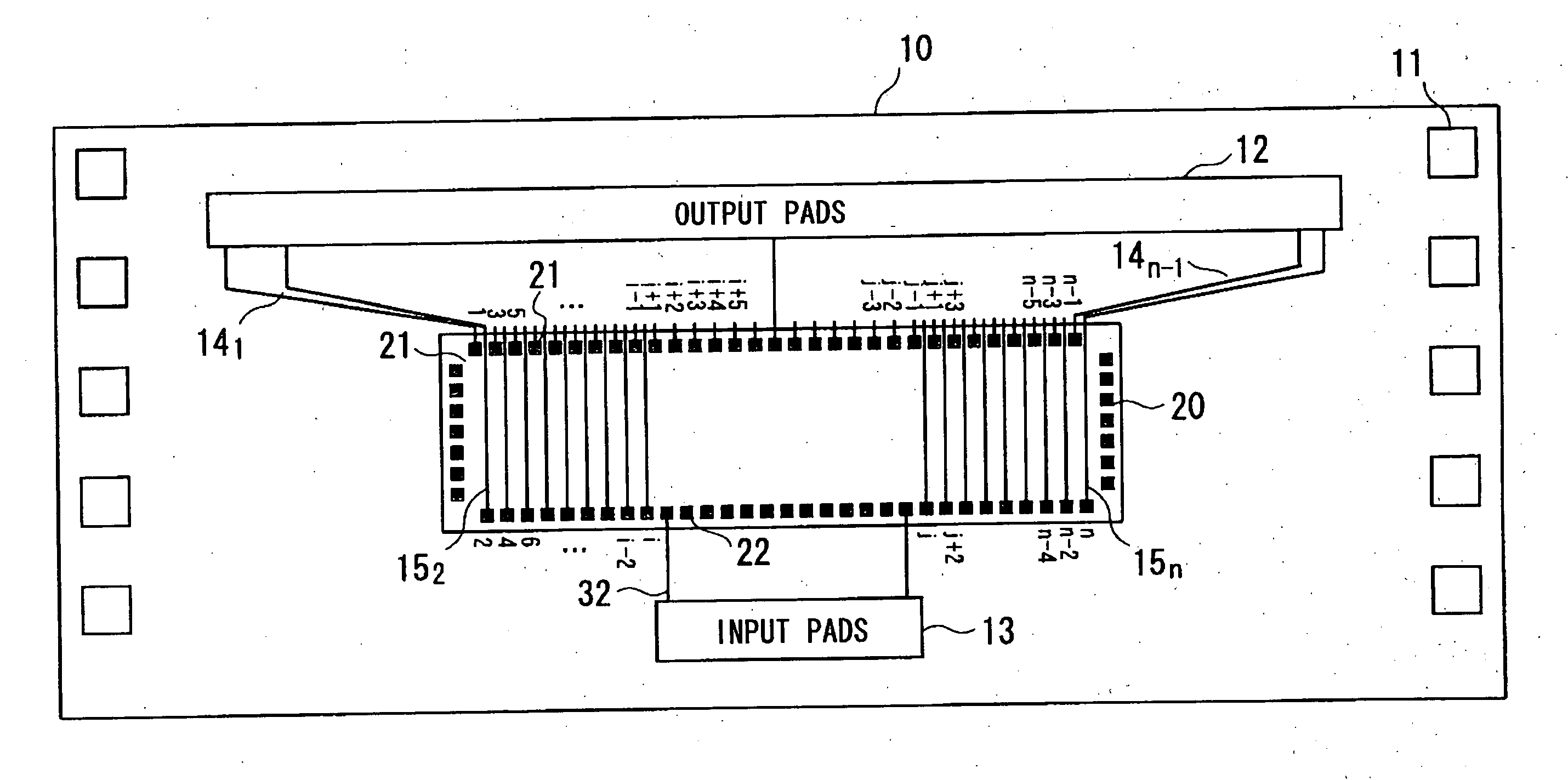
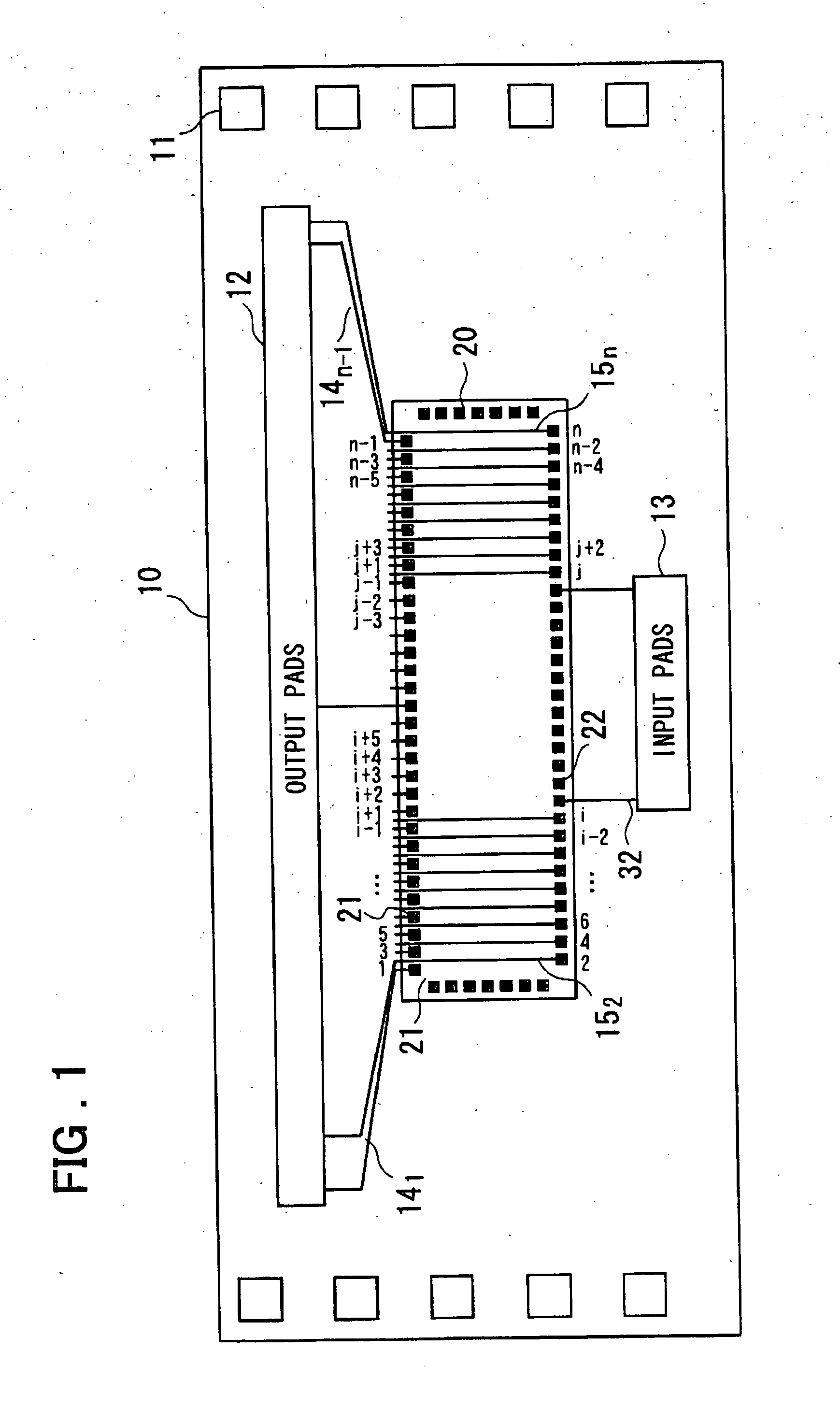
[0099] Preferred embodiments of the present invention will be described with reference to drawings. Referring to FIG. 1, a semiconductor device according to an embodiment of the present invention includes a substrate (10), a plurality of signal output pads (12) provided on the substrate (10), a plurality of signal input pads (13) provided on the substrate (10), a display driver IC (20)(a data driver or a gate driver) which has input terminals thereof connected to the signal input pads (13) and output terminals thereof connected to the signal output pads (12). As an example, the display driver IC (20) includes first, third, fifth, . . . , (i+1)th, . . . , (n−1)th output terminals on a first side of the display driver IC (20) facing the signal output pads (12). A second side on the opposite side of the first side faces the signal input pads (13), and at least one segment of the second side includes a plurality of input terminals (22), and at least one portion of the remaining segments...


PUM


Abstract

Disclosed is a device which comprises a substrate, a plurality of signal output terminal electrodes provided on the substrate, a plurality of signal input terminal electrodes provided on the substrate, and a display driver IC having input terminals thereof connected to the signal input terminal electrodes and output terminals thereof connected to the signal output terminal electrodes. A plurality of output terminals (first, third, fifth, . . . (i+1)th, and (n−1)th) are included on a first side of the display driver IC facing the signal input terminal electrodes. A second side on an opposite side of the first side faces the signal input terminal electrodes. Input terminals 22 are included in at least one segment of the second side, and output terminals (second, fourth, sixth, ith, jth, (j+2)th, (n−2)th, and nth) are included in at least one portion of the remaining segment of the second side. One output terminal on the second side passes between two of the output terminals on the first side that correspond to the one output terminal and is connected to a corresponding one of the signal output terminal electrodes through a corresponding one of wiring that passes through the underside of the display driver IC.

Description

FIELD OF THE INVENTION [0001] The present invention relates to an IC (Integrated Circuit) for driving a display device. More specifically, the invention relates to a configuration suitable for being applied to a semiconductor device having output terminals for driving on two or more sides of the IC chip thereof for driving the display device, and the display device provided with the semiconductor device. BACKGROUND OF THE INVENTION [0002] Among display device driver circuits, data driver circuits (also referred to as “source drivers”) include driver circuits each for driving a data line of a display panel (LCD (Liquid Crystal Display) panel, an EL (Electro Luminescence) panel, or the like) in parallel, corresponding to data lines for each line, for example. The data driver circuit inputs a digital video signal from a host device such as a CPU, for example, converts the digital video signal to a gray-scale voltage / current corresponding to the digital video signal, and drives the data...

Claims


Application Information

Patent Timeline
Patent Type & Authority Applications(United States)
IPC IPC(8): H01L23/48
CPCG02F1/13452H01L2224/73204H01L2224/32225H01L2224/16225H01L2924/00
Inventor TSUKIJI, MASAHARU
Owner RENESAS ELECTRONICS CORP
Why Eureka
Try Eureka