
Eureka
For R&D, Eureka makes reading and utilizing patents & technical documents easy.
Eureka AIR
Designed for self-driven R&D workflows. Generate viable solutions, solve complex R&D challenges, empower your innovation with AI.

Eureka Materials
Designed for material experts only. Revolutionize your material R&D, from search, analyze, to developing new materials.

TechResearch
Generate reliable direction feasibility study reports for your R&D in just a few steps.

TechSeek
Discover and master advanced knowledge NOW. Basics, ideas, possibilities, all at once.

TechMind
As an expert in R&D Theories, TechMind can generates customized viable solutions instantly.

TechRisk
Analyze your overall solution with one click, know your potential R&D risks in advance.

TechMonitor
Get weekly tech updates, stay abreast of the latest tech innovations and key insights.
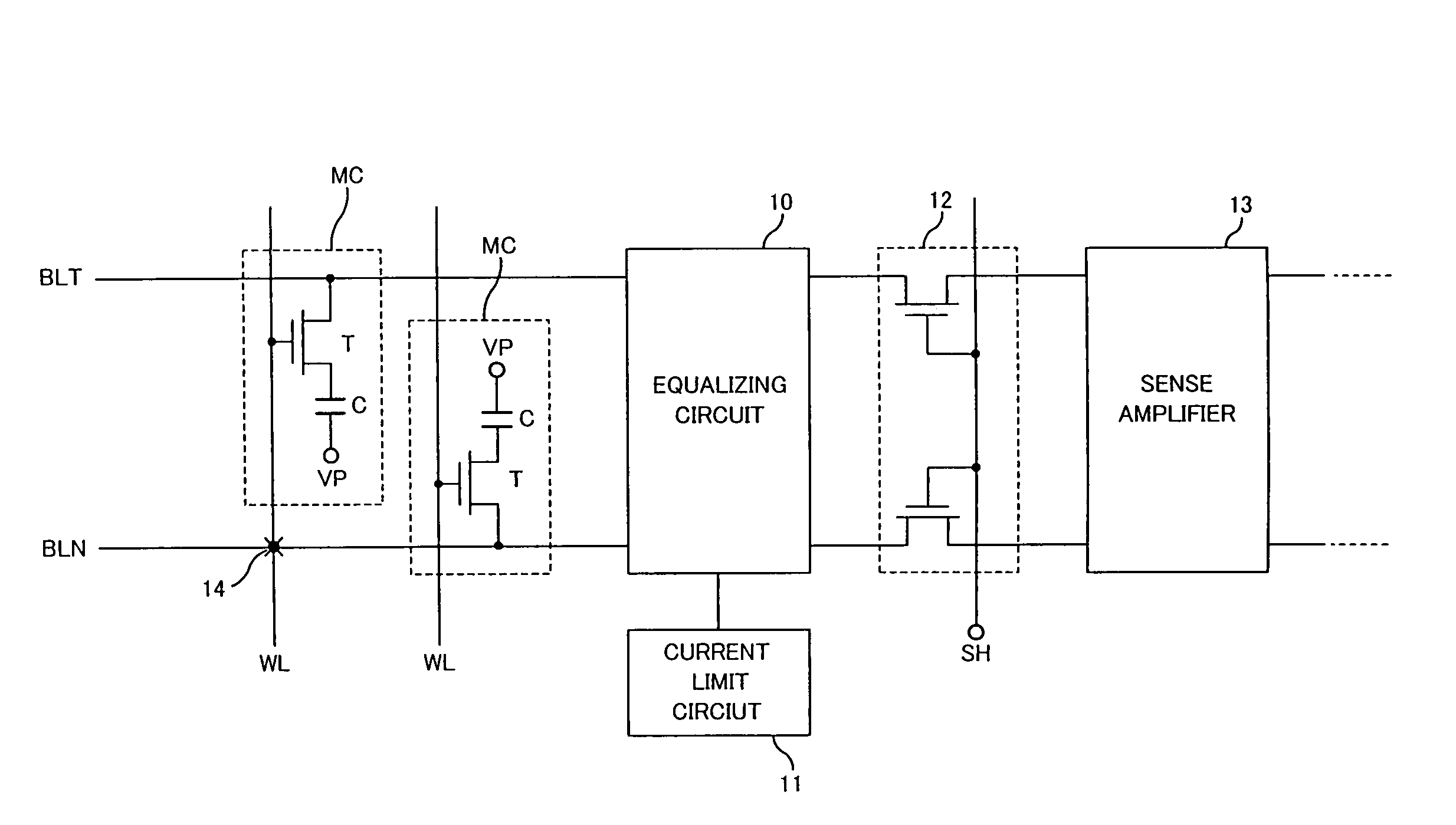
Current limit circuit and semiconductor memory device
- Summary
- Abstract
- Description
- Claims
- Application Information
AI Technical Summary
Benefits of technology
Problems solved by technology
Method used
Image

Examples
first embodiment
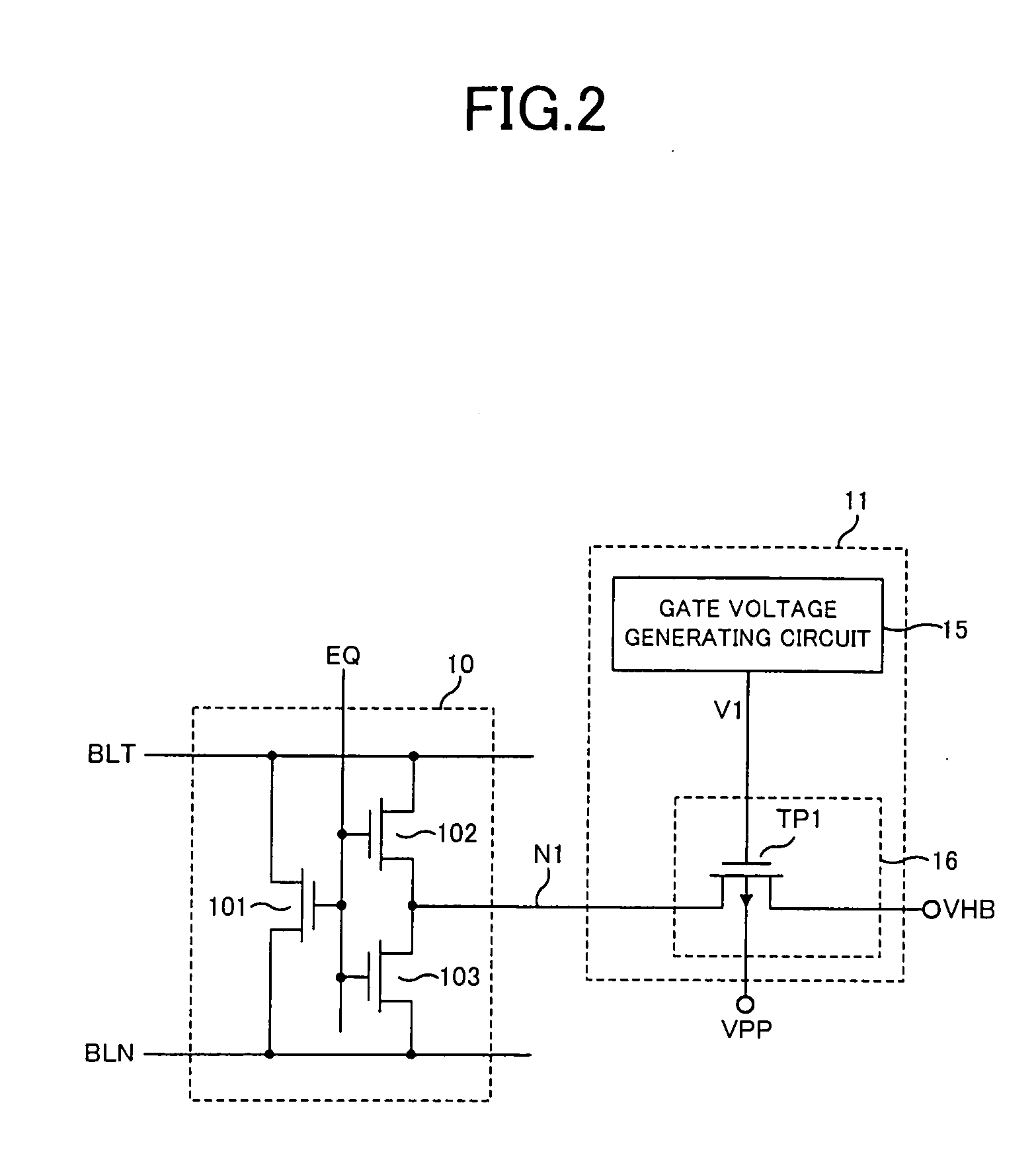
[0058]FIG. 4 is a graph showing the subthreshold characteristics of the PMOS transistor TP1 of FIG. 2 in a state where the voltage V1 is controlled based on the configuration of the gate voltage generating circuit 15 of the Herein, to compare with FIG. 11, three types of characteristics C1, C2, C3 as shown in FIG. 11 are assumed to be fluctuations in the threshold voltage Vtp, and the VHB is assumed to be set to 0.6 V. The vertical axis of the graph represents the logarithm of the absolute value |IDS|, and the horizontal axis represents both the gate-source voltage VGS and the voltage V1.
[0059] First, an operation point B1 in the characteristic C1 corresponding to Vtp=−1.0 V coincides with the operation point A1 in FIG. 11. Here, a case is considered in which the absolute value of the threshold voltage Vtp decreases starting from the operation point B1, shifting to the characteristic C2 (Vtp=−0.9 V) In this case, as distinct from FIG. 11 in which the voltage V0 is fixed, since the ...
second embodiment
[0067] In the second embodiment, a configuration is shown in which the limiting current can be changed using the variable resistor R2, but the limiting current can be changed by other methods. For example, it is possible to switch the level of the reference voltage VREF1 in the test mode.
[0068] Next, a third embodiment of the gate voltage generating circuit 15 will be described below based on a configuration of FIG. 8. As shown in FIG. 8, in the gate voltage generating circuit 15 of the third embodiment, a configuration of a level detection circuit 25 is different from that of the a level detection circuit 20 of the first embodiment. That is, a series circuit where a a PMOS transistor TP3 and a resistor R3 are connected to each other at node N4 as an intermediate node is formed, and the connection relationship is inverse to that of the first embodiment. The PMOS transistor TP3 has a source to which the bit line pre-charge voltage VHB is applied, and drain and gate connected to node ...
third embodiment
[0075]FIG. 9 is a graph showing subthreshold characteristics of the PMOS transistor TP1 corresponding to FIG. 4 in a state where the voltage V1 is controlled based on the configuration of the gate voltage generating circuit 15 of the Three types of characteristics C1, C2, C3 shown in FIG. 9 and conditions of the graph notation are the same as in FIG. 4, and descriptions thereof are omitted.
[0076] The graph of FIG. 9 is approximately the same as the graph of FIG. 4, except that three operation points B1′, B2′, B3′ corresponding to characteristics C1, C2, C3 are slightly shifted from three operation points B1, B2, B3 in FIG. 4, respectively. This reflects that the limiting current fluctuates slightly due to the influence of the threshold voltage Vtp. However, comparing the graph of FIG. 9 with the graph of FIG. 11, changes in |IDS| are remarkably small at least as compared with three operation points A1, A2, A3 in FIG. 11, and it is understood that a sufficient effect can be obtained...
PUM
 Abstract
Description
Claims
Application Information
 - R&D Engineer
- R&D Manager
- IP Professional
- Industry Leading Data Capabilities
- Powerful AI technology
- Patent DNA Extraction
Browse by: Latest US Patents, China's latest patents, Technical Efficacy Thesaurus, Application Domain, Technology Topic, Popular Technical Reports.
© 2024 PatSnap. All rights reserved.Legal|Privacy policy|Modern Slavery Act Transparency Statement|Sitemap|About US| Contact US: help@patsnap.com