
Semiconductor integrated circuit device

a technology of integrated circuits and semiconductors, applied in the direction of generating/distributing signals, instruments, sustainable buildings, etc., can solve the problems of long clock wiring length, clock skew, etc., to reduce the number of clock gating circuits, the effect of reducing the power consumption of clock signals

Inactive Publication Date: 2007-01-11
PANASONIC CORP
View PDF9 Cites 3 Cited by
  • Summary
  • Abstract
  • Description
  • Claims
  • Application Information

AI Technical Summary

Benefits of technology

[0009] An object of this invention is to provide a semiconductor integrated circuit device capable of minimizing the clock skew and reducing power consumption by a clock signal.

Problems solved by technology

In a large-scaled semiconductor integrated circuit device, problematic is a propagation delay time difference (clock skew) of a clock signal on a wiring path from a clock supply point to a clock input of a clock synchronizing circuit gate such as a flip-flop operating in synchronism with the clock supplied.
Increased clock skew makes it impossible to operate the semiconductor integrated circuit device at a high speed.
However, in the clock supply to the grid-like wring structures, the entire wiring length of the clock wirings is very long, and the clock supply to each the grid-like wiring structures is always executed.
This gives rise to a problem that the power consumption by clocks is greatly increased.
However, the wiring lengths from the clock input in the semiconductor integrated circuit device to the grid-like wiring structures of the function modules are different, thereby giving a tendency of increasing the clock skew.
In such a wiring structure, the reduction of the clock skew is limited thereby to present a problem of restraining the high speed operation of the semiconductor integrated circuit device.
As described above, the conventional semiconductor integrated circuit device has a limit in the aspect of reducing the clock skew and power consumption by clocks.
So it is difficult to operate the semiconductor integrated circuit device at a high speed by reduction of the clock skew and reduce the power consumption in the semiconductor integrated circuit device.

Method used


Image

  • Semiconductor integrated circuit device
  • Semiconductor integrated circuit device
  • Semiconductor integrated circuit device

Examples


embodiment 1

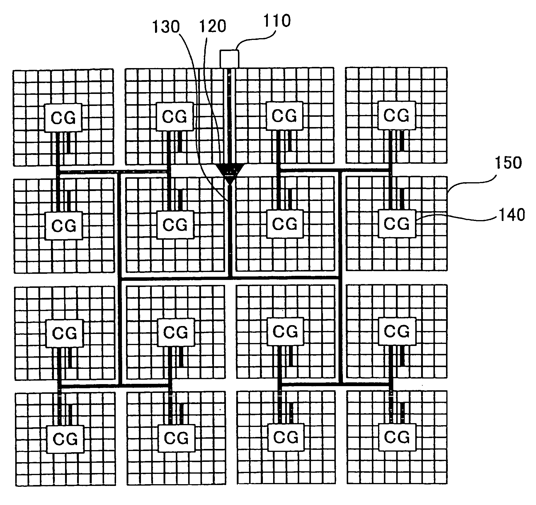
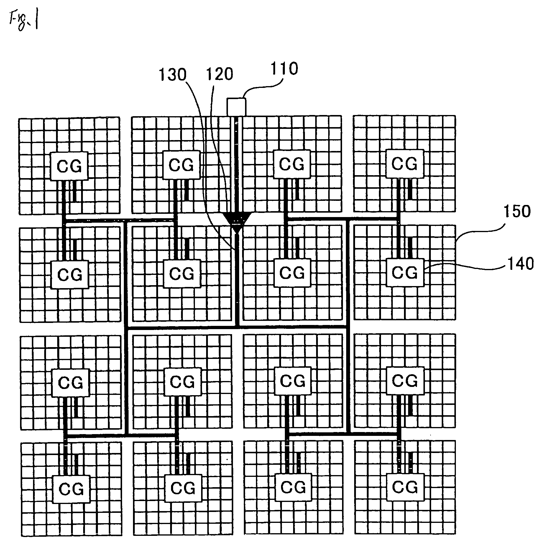
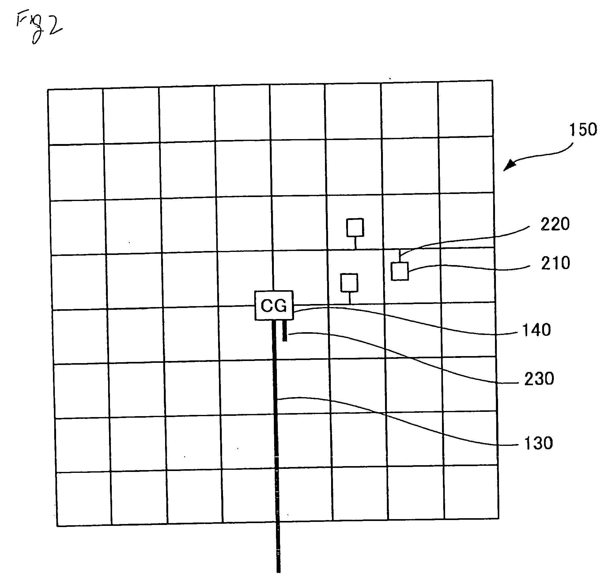
[0033]FIG. 1 is a view showing the clock wiring structure of a semiconductor integrated circuit device according to the first embodiment of this invention. In FIG. 1, reference numeral 110 denotes a clock input to the semiconductor integrated circuit device; 120 a buffer gate which is a buffer circuit serving as a clock driver; 130 a first wiring structure; 140 one of clock gating circuits; and 150 one of grid-like wiring structures in the unit regions.

[0034] The first wiring structure 130 is a wiring structure in which the clock input 110 is connected to a plurality of grid-like wiring structures 150 with equal wiring lengths. In FIG. 1, the clock input 110 is connected to the clock inputs to the clock gating circuits 140 located in the plurality of grid-like wiring structures with substantially equal wiring lengths by an equal-length branched wiring structure with H-shapes via the buffer gate 120 inserted on the way of wiring paths. The outputs from the clock gating circuits 140 ...

embodiment 2

[0059]FIG. 7 is a view showing the clock wiring structure in the semiconductor integrated circuit device according to the second embodiment of this invention. In the first wiring structure 130 connecting the clock input 110 and the plurality of grid-like wiring structures 140 with equal wiring lengths, the outputs from the clock gating circuits 140 are connected to a region consisting of a plurality of grid-like wiring structures 150 so that the supply and stop of clocks to the plurality of grid-like wiring structures 150 are simultaneously gate-controlled.

[0060] For this reason, the positions where the clock gating circuits 140 are inserted in the first wiring structure are different from those in the first embodiment. Specifically, the clock gating circuits 140 are located on the symmetrically center line of the region 710. Their outputs are connected to the plurality of grid-like wiring structures 150 through the buffer gate(s) at a necessary number of stage(s).

[0061] More spec...


PUM


Abstract

The semiconductor integrated circuit device includes a plurality of grid-like wiring structures 150 arranged as unit regions in an entire circuit area and having the same shape as a clock wiring structure, respectively; a first wiring structure in which the wiring paths from an clock input 110 to the respective grid-like wiring structures 150 are connected with substantially equal lengths and a common buffer circuit 120 or buffer circuits with the same kind and the same number of stages and clock gating circuits 140 are inserted in the same order in the respective wiring paths; and a second wiring structure connecting a clock synchronizing circuit to the grid-like wiring structure with the shortest length in each unit region. The clock is gate-controlled by a clock control signal separately supplied to the clock gating circuit.

Description

BACKGROUND OF THE INVENTION [0001] 1. Field of the Invention [0002] This invention relates to a semiconductor integrated circuit device capable of realizing minimization of clock skew and low power consumption. [0003] 2. Description of the Related Art [0004] In a large-scaled semiconductor integrated circuit device, problematic is a propagation delay time difference (clock skew) of a clock signal on a wiring path from a clock supply point to a clock input of a clock synchronizing circuit gate such as a flip-flop operating in synchronism with the clock supplied. Increased clock skew makes it impossible to operate the semiconductor integrated circuit device at a high speed. Therefore, in a conventional semiconductor integrated circuit device, as a wiring structure for supplying the clock to the clock synchronizing circuit gate, using an equal-length branched wiring structure with H-shapes and grid-like wiring structures represented by mesh-like wirings composed of orthogonally crossin...

Claims


Application Information

Patent Timeline
Patent Type & Authority Applications(United States)
IPC IPC(8): G06F17/50
CPCG06F1/10Y02B60/1221G06F1/3237G06F1/3203Y02D10/00
Inventor NISHIKAWA, RYOTA
Owner PANASONIC CORP
Learn More