Image sensor with SOI substrate

a technology of image sensor and substrate, applied in the field of image sensor, can solve the problems of difficult integration of image sensor array into soi technology, poor signal-to-noise ratio, poor dynamic range of cmos imager, etc., and achieve the effect of reducing dark current and large fill factor

Active Publication Date: 2007-01-18
APTINA IMAGING CORP
View PDF17 Cites 68 Cited by
  • Summary
  • Abstract
  • Description
  • Claims
  • Application Information

AI Technical Summary

Benefits of technology

[0009] An exemplary embodiment of the invention includes a CMOS imager (i.e., image sensor) pixel that utilizes a silicon-on-insulator, i.e., SOI, substrate and a photosensor (e.g., pinned photodiode) that substantially spans the pixe...

Problems solved by technology

CMOS imagers typically suffer from poor signal to noise ratios and poor dynamic range as a result of the inability to fully collect and store the electric charge collecte...

Method used


Image

  • Image sensor with SOI substrate
  • Image sensor with SOI substrate
  • Image sensor with SOI substrate

Examples


Embodiment Construction

[0025] Although this invention will be described in terms of certain exemplary embodiments, other embodiments will be apparent to those of ordinary skill in the art, which also are within the scope of this invention. Accordingly, the scope of the invention is defined only by reference to the appended claims.

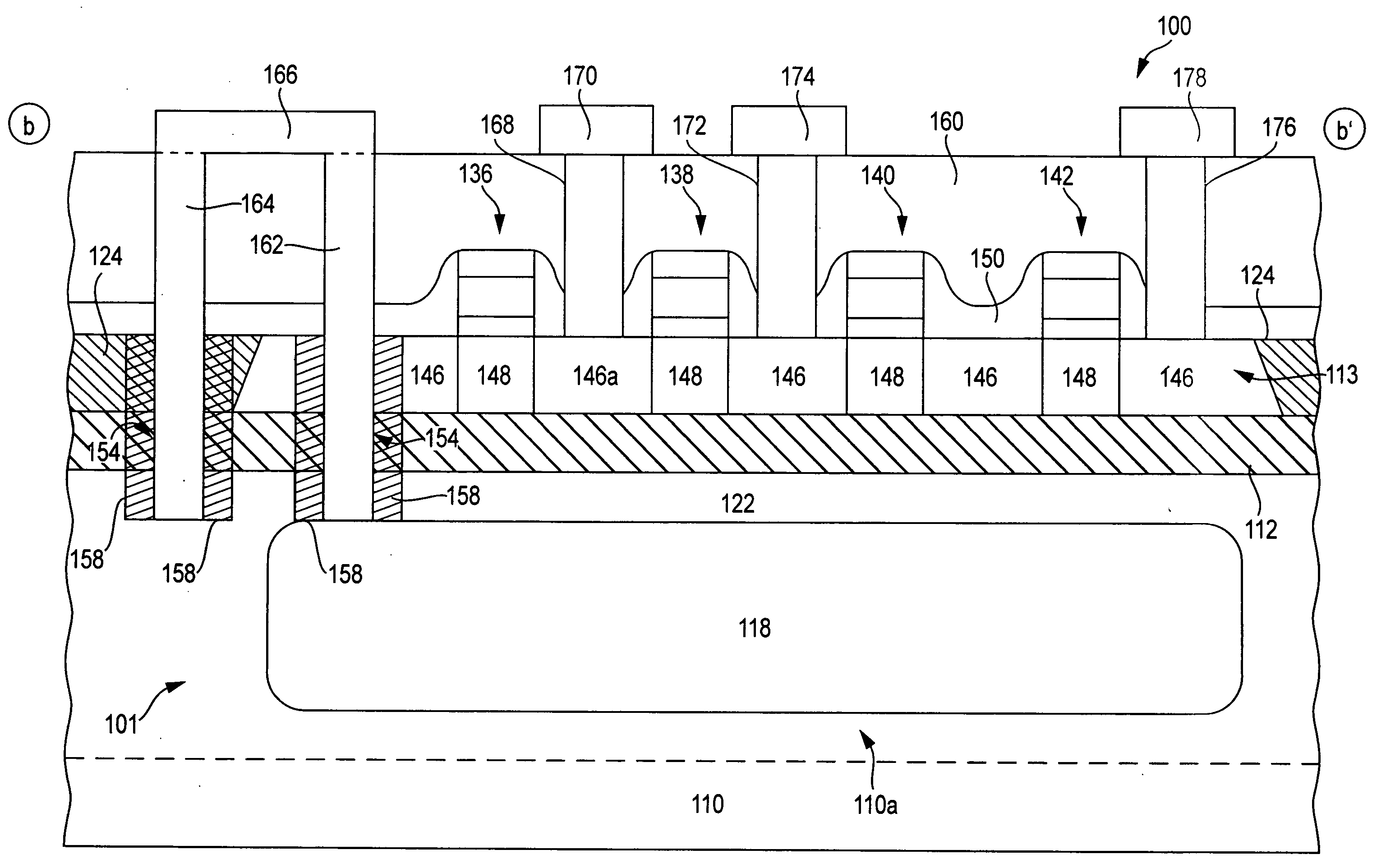
[0026] The terms “substrate” or “wafer” are used interchangeably in the following description. A silicon-on-insulator (SOI) substrate is used in accordance with the invention, which may also include epitaxial layers of silicon supported by a base semiconductor foundation. When reference is made to a substrate or wafer in the following description, previous process steps may have been utilized to form regions or junctions in or over a base semiconductor or foundation.

[0027] The term “pixel” refers to a photo-element unit cell containing a charge accumulating photoconversion device and associated transistors for converting electromagnetic radiation to an electrical signal. The pi...


PUM


Abstract

An imager pixel utilizing a silicon-on-insulator substrate, a photodiode in said substrate below the buried oxide, and a dual contact to said photodiode and methods of forming said imager pixel. The photodiode has an increased fill factor due to its increased size relative to the pixel.

Description

FIELD OF THE INVENTION [0001] The invention relates to imager technology. In particular, the invention relates to imager devices with an SOI substrate. BACKGROUND OF THE INVENTION [0002] CMOS imagers are known in the art. Exemplary CMOS imaging circuits, processing steps thereof, and detailed descriptions of the functions of various CMOS elements of an imaging circuit are described, for example, in U.S. Pat. No. 6,140,630, U.S. Pat. No. 6,376,868, U.S. Pat. No. 6,310,366, U.S. Pat. No. 6,326,652, U.S. Pat. No. 6,204,524, and U.S. Pat. No. 6,333,205, each assigned to Micron Technology, Inc. The disclosures of the forgoing patents are hereby incorporated by reference in their entirety. [0003] A top-down and cross-sectional view of a typical and exemplary CMOS four-transistor (4T) pixel cell 10 is illustrated in FIGS. 1a and 1b. As it will be described below, the CMOS sensor pixel 10 includes a photoconversion device 12 (e.g., photo-generated charge accumulating area) in a portion of t...

Claims


Application Information

Patent Timeline
IPC IPC(8): H01L31/113
CPCH01L27/14603H01L27/14609H01L27/14689H01L27/14636H01L27/14645H01L27/1463
Inventor MOULI, CHANDRA
Owner APTINA IMAGING CORP
Why Eureka
Try Eureka