Electro-optical device and method for manufacturing the same

a technology of optical devices and optical components, applied in semiconductor devices, instruments, electrical apparatus, etc., can solve the problems of low production yield of display, low reliability of connections, and conventional displays, and achieve the effects of enhancing carrier mobility, enhancing carrier mobility, and elevating the degree of anchoring

Inactive Publication Date: 2007-01-25
SEMICON ENERGY LAB CO LTD
View PDF99 Cites 115 Cited by
  • Summary
  • Abstract
  • Description
  • Claims
  • Application Information

AI Technical Summary

Benefits of technology

[0032] In the semi-amorphous semiconductors, the carrier mobility increases with elevating degree of anchoring. To enhance carrier mobility and to allow the crystalli...

Problems solved by technology

Thus, because of the construction as described hereinabove, a conventional display suffers problems as follows:
(3) The connections are of low reliability.
(4) The production yield of the display is low.
(5) The production cost is increased.
Since the peripheral circuit portion comprises a very complicated device structure, the circuit patter...

Method used


Image

  • Electro-optical device and method for manufacturing the same
  • Electro-optical device and method for manufacturing the same
  • Electro-optical device and method for manufacturing the same

Examples


example 1

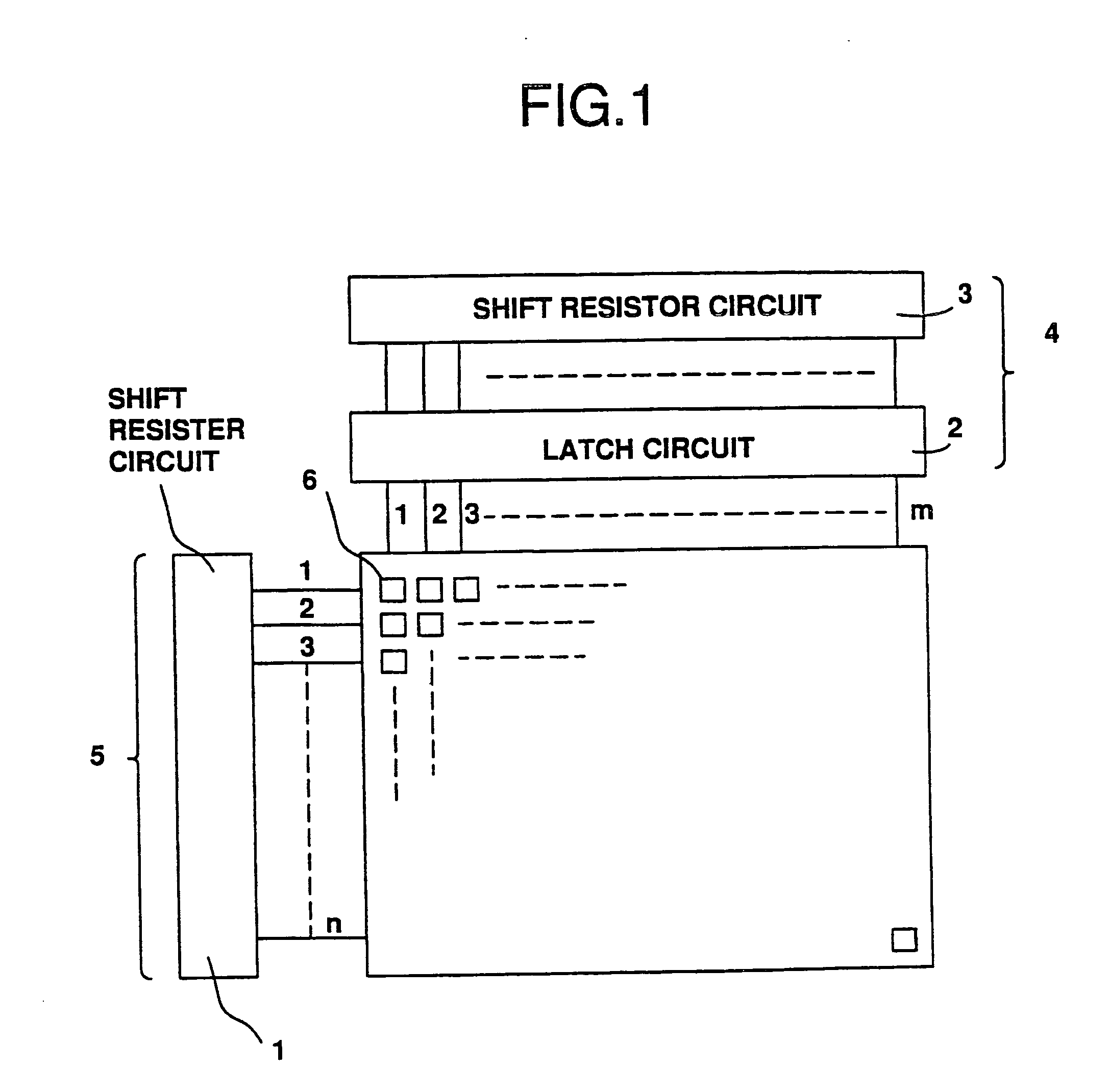
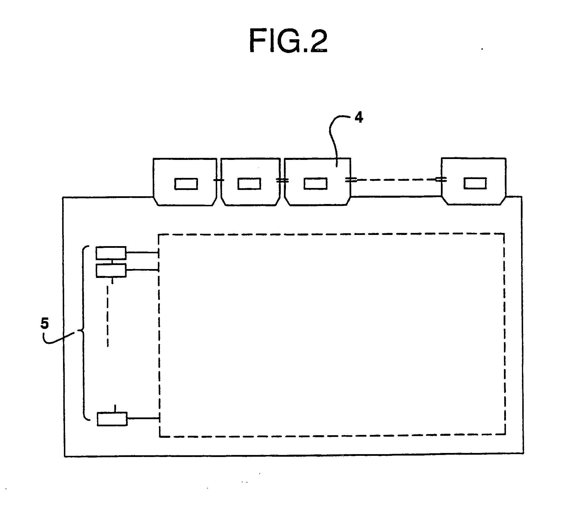
[0043] Referring to FIG. 1, a liquid crystal display device having an m×n circuit structure is described. In FIG. 2 is also given the outer appearance of the liquid crystal display device. In FIG. 1, a shift resister circuit portion 1 (a means for supplying a signal to a wiring of the X direction) being connected to a wiring of the X direction is solely fabricated as TFTs 5 in a similar manner as an active device provided to a pixel 6, and a peripheral circuit portion (a means for supplying a signal to a wiring of the Y direction) connected to a wiring of the Y direction is provided as ICs 4 which is connected to the substrate by TAB. The thin film transistors provided in the pixel 6 as the active device and the thin film transistors 5 constituting the shift resister circuit portion 1 are provided on a single substrate.

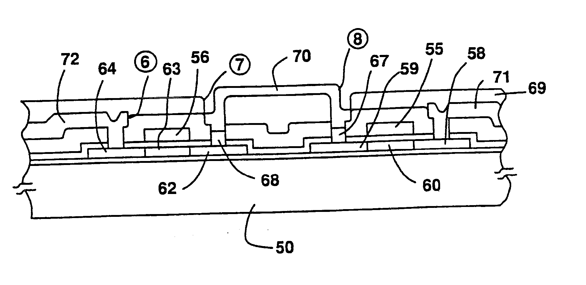
[0044] The actual arrangement of the electrodes and the like corresponding to this circuit structure is shown in FIG. 6. In FIG. 6, however, the structure is simplif...

example 2

[0069] In FIG. 7 is given a schematic view of a liquid crystal display device according to another embodiment of the present invention. The basic circuits and the like are the same as those employed in the liquid crystal display device described in Example 1. Referring to FIG. 7, the peripheral circuit connected to the wirings for the Y direction is constructed with ICs 4, and the ICs 4 are directly provided on the substrate by a COG method.

[0070] The pad electrodes of the ICs 4 can be connected with the wirings of the Y direction at a narrower interval by the use of a COG method instead of the TAB method. Thus, the process of the present example enables a finer display pixel design. Furthermore, since the ICs are provided on the substrate, the total volume of the display device remains almost unchanged to give a thinner liquid crystal display device.

example 3

[0071] Referring to FIG. 8, a liquid crystal display device having an m×n circuit structure is described below. Among the peripheral circuit portions (a means for supplying a signal to wirings of the X direction) connected to the wirings of the X direction, only an analog switch array circuit portion 1 is fabricated as TFTs in the same process as that used for fabricating the active device provided to a pixel 6. Furthermore, only an analog switch array circuit portion 2 in the peripheral circuit portion (a means for supplying a signal to wirings of the Y direction) connected to the wirings of the Y direction is also fabricated as TFTs, while providing the rest of the peripheral circuit portion by making them into ICs 4 having connected to a substrate using a COG method. The peripheral circuit portion provided as TFTs is in a CTFT structure (complementary structure) similar to the active device established to the pixels.

[0072] In FIG. 6 is provided the actual arrangement of the elec...


PUM


Abstract

An electro-optical device and a method for manufacturing the same are disclosed. The device comprises a pair of substrates and an electro-optical modulating layer (e.g. a liquid crystal layer having sandwiched therebetween, said pair of substrates consisting of a first substrate having provided thereon a plurality of gate wires, a plurality of source (drain) wires, and a pixel matrix comprising thin film transistors, and a second substrate facing the first substrate, wherein, among the peripheral circuits having established on the first substrate and being connected to the matrix wirings for the X direction and the Y direction, only a part of said peripheral circuits is constructed from thin film semiconductor devices fabricated by the same process utilized for an active device, and the rest of the peripheral circuits is constructed from semiconductor chips. The liquid crystal display device according to the present invention is characterized by that the peripheral circuits are not wholly fabricated into thin film transistors, but only those portions having a simple device structure, or those composed of a small number of devices, or those comprising an IC not easily available commercially, or those comprising an expensive integrated circuit, are fabricated by thin film transistors. According to the present invention, an electro-optical device is provided at an increased production yield with a reduced production cost.

Description

BACKGROUND OF THE INVENTION [0001] 1. Field of the Invention [0002] The present invention relates to an electro-optical device which comprises thin film transistors (referred to hereinafter as TFTs) and to a method for manufacturing such a device. [0003] 2. Description of the Prior Art [0004] More attention is now paid to flat displays than to CRTs (cathode ray tubes) for use in office automation (OA) machines and the like, and particularly, there is an increasing demand for large-area display devices. There is also an active and rapid development in the application field of flat displays such as wall television (TV) sets. Furthermore, there are demands for color flat displays and finer display images. [0005] A liquid crystal display device is known as a representative example of a flat display. A liquid crystal display device comprises a pair of glass substrates having incorporated therebetween a liquid crystal composition together with electrodes, and the images are displayed by t...

Claims


Application Information

Patent Timeline
IPC IPC(8): H01L29/04
CPCH01L27/124G02F1/13454
Inventor YAMAZAKI, SHUNPEI
Owner SEMICON ENERGY LAB CO LTD
Why Eureka
Try Eureka