High electron mobility electronic device structures comprising native substrates and methods for making the same

Inactive Publication Date: 2007-01-25
CREE INC
View PDF99 Cites 82 Cited by
  • Summary
  • Abstract
  • Description
  • Claims
  • Application Information

AI Technical Summary

Benefits of technology

[0010] The present invention relates to electronic device structures including high quality III-nitride layers grown on native insulating III-V substrates and at least one terminal comprising a conductive materi

Problems solved by technology

Despite the use of nucleation layers, crystal quality of an epitaxial device layer grown on a foreign substrate is inferior to the epitaxial device layer that would be grown on a crystalline native substrate.
Due to the inferiority of epitaxial device layers grown on foreign substrates, the intrinsic material potential of AlGaN/GaN systems is not realized in conventional HEMTs.
Surprisingly, Applicants have found that when homoepitaxial GaN layers are grown on native SI GaN substrates using conventional m

Method used


Image

  • High electron mobility electronic device structures comprising native substrates and methods for making the same
  • High electron mobility electronic device structures comprising native substrates and methods for making the same
  • High electron mobility electronic device structures comprising native substrates and methods for making the same

Examples


example 1

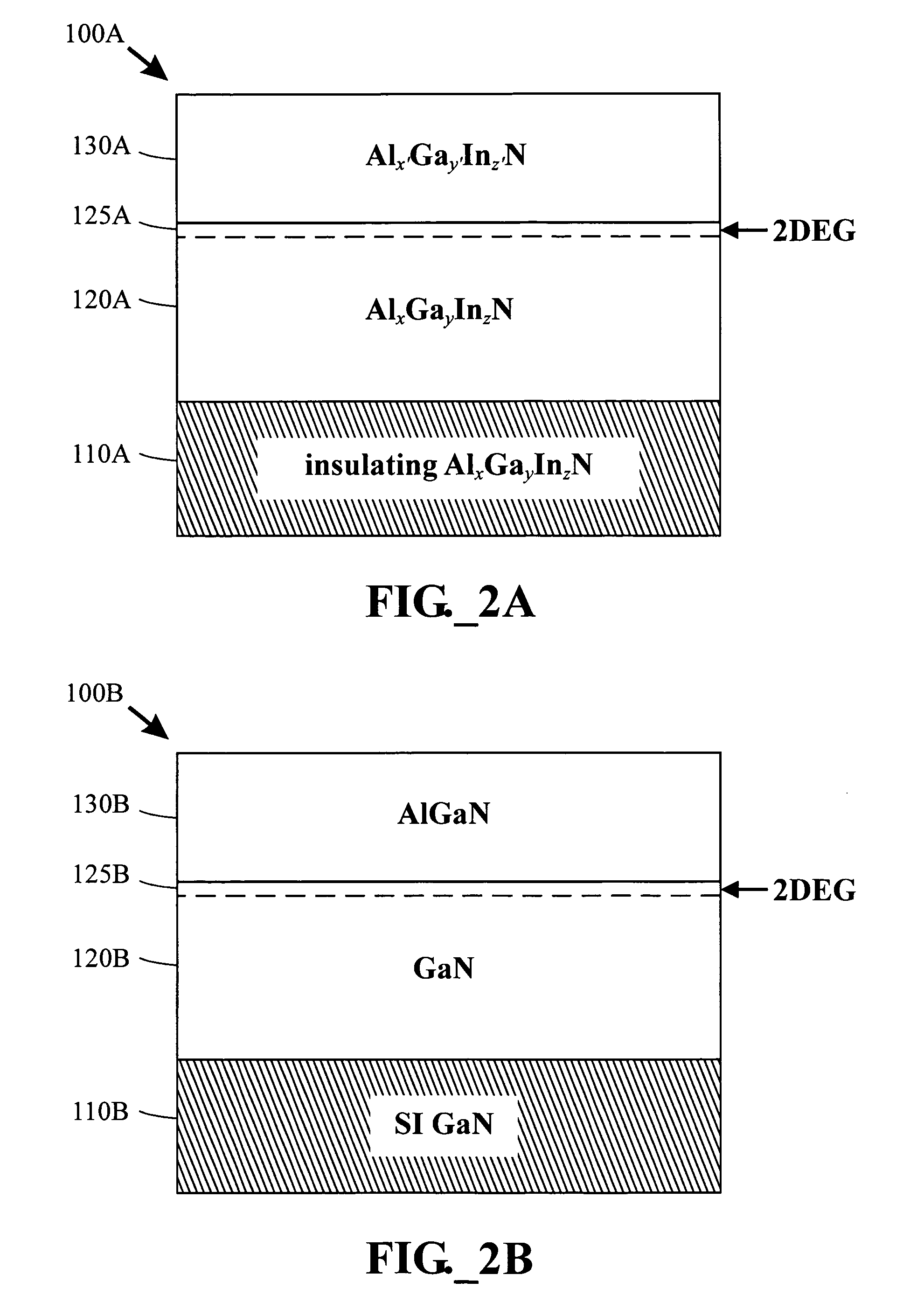
[0064] A first III-nitride multi-layer device structure of the type shown schematically in FIGS. 2A-2B was constructed with a c-plane SI GaN substrate. The structure was grown by MOCVD using ammonia as the nitrogen source and TMG (trimethylgallium) and TMA (trimethylaluminum) as the gallium and aluminum sources, respectively. A cleaned, c-plane SI GaN substrate was loaded into a reactor and heated to the growth temperature. Growth began once the reactor reached the growth temperature, without anneal or nucleation steps. A 100 nm thickness first GaN layer was grown on the substrate with the following process conditions: a susceptor temperature of 1220C (note that substrate temperature is typically about 50-200C lower than the susceptor temperature), a growth pressure of 100 mbar, and a growth rate of about 2 μm / hr. The aluminum source was then turned on and a 10 nm thickness second AlGaN layer was grown on the first layer with the percentage of Al in the second layer being about 24% ...

example 2

[0065] A second III-nitride multi-layer device structure of the type shown schematically in FIGS. 2A-2B was constructed with a vicinal SI GaN substrate. The structure was grown by MOCVD using ammonia as the nitrogen source, TMG as the gallium source, and TMA as the aluminum source. A cleaned, vicinal SI GaN substrate was loaded into a reactor and heated to the growth temperature. The vicinal substrate was offcut by 1 degree toward the direction. Growth began once the reactor reached the growth temperature, without anneal or nucleation steps. A 50 nm thickness first GaN layer was grown on the substrate with the following process conditions: a susceptor temperature of 1170C, a growth pressure of 100 mbar, and a growth rate of about 2 μm / hr. The aluminum source was then turned on and a 10 nm thickness second AlGaN layer was grown on the first layer with the percentage of Al in the second layer being about 24% of the metal in the nitride allow. The aluminum and gallium sources were the...

example 3

[0066] A III-nitride multi-layer structure of the type shown schematically in FIG. 5 (i.e., including a GaN cap layer) was constructed. The structure was grown by MOCVD using ammonia as the nitrogen source, TMG as the gallium source, and TMA as the aluminum source. A cleaned, c-plane SI GaN substrate was loaded into a reactor and heated to the growth temperature. Growth began once the reactor reached the growth temperature, without anneal or nucleation steps. The growth conditions for all layers were: a susceptor temperature of 1170C, a growth pressure of 100 mbar, and a growth rate of about 2 μm / hr. The initial growth was that of a 100 nm thickness first GaN layer on the substrate. The aluminum source was then turned on and a 22 nm thickness second AlGaN layer was grown on the first layer, with the percentage of Al in the second layer being about 27% of the metal in the nitride alloy. The aluminum source was then turned off, and a 2 nm thickness third GaN cap layer was grown on the...


PUM


Abstract

An electronic device structure comprises a substrate layer of semi-insulating AlxGayInzN, a first layer comprising AlxGayInzN, a second layer comprising Alx′Gay′Inz′N, and at least one conductive terminal disposed in or on any of the foregoing layers, with the first and second layers being adapted to form a two dimensional electron gas is provided. A thin (<1000 nm) III-nitride layer is homoepitaxially grown on a native semi-insulating III-V substrate to provide an improved electronic device (e.g., HEMT) structure.

Description

GOVERNMENT RIGHTS IN INVENTION [0001] Work relevant to the subject matter hereof was conducted in the performance of DARPA Contract No. N00014-02-C-0321. The United States government may have certain rights in this invention.FIELD OF THE INVENTION [0002] The present invention relates to electronic device (e.g., high electron mobility transistor) structures including III-nitride device layers grown on native insulating substrates and methods for making the same. DESCRIPTION OF THE RELATED ART [0003] Gallium nitride and related III-V alloys have exhibited great potential for high power and / or high frequency electronic applications. Particularly desirable applications include high electron mobility transistors (HEMTs), which are electronic devices having three terminals including a gate, a drain, and a source. Electric potential on the gate controls the current flow between the source and the drain. AlGaN / GaN heterostructure-based HEMTs are of interest because a two-dimensional electro...

Claims


Application Information

Patent Timeline
IPC IPC(8): H01L29/732
CPCH01L29/2003H01L29/7787H01L29/66462
Inventor BRANDES, GEORGE R.XU, XUEPINGDION, JOSEPHVAUDO, ROBERT P.FLYNN, JEFFREY S.
Owner CREE INC
Why Eureka
Try Eureka