Nanoimprint lithograph for fabricating nanoadhesive

a nano-adhesive and nano-print technology, applied in the field of nanotechnology, can solve the problems of not meeting the requirements of low production cost and mass production, the current throughput of the technique is too low to be economically practical for mass production, and the mask technology and exposure system are currently rather complex and expensive, and achieve the effect of low cos

Inactive Publication Date: 2007-01-25
CONTREL TECH CO LTD
View PDF6 Cites 58 Cited by
  • Summary
  • Abstract
  • Description
  • Claims
  • Application Information

AI Technical Summary

Benefits of technology

[0012] As the steps indicated above, the nanoadhesive can be produ

Problems solved by technology

While the scanning electron beam lithography demonstrated 10-nm resolution, it exposes point by point in a serial manner and thus, the current throughput of the technique is too low to be economically practical for mass production.
The x-ray lithography demonstrated 20-nm resolution in a contact printing mode and has a high

Method used


Image

  • Nanoimprint lithograph for fabricating nanoadhesive
  • Nanoimprint lithograph for fabricating nanoadhesive
  • Nanoimprint lithograph for fabricating nanoadhesive

Examples


Embodiment Construction

[0025] Referring to FIGS. 1-7, a nanoimprint lithography method of fabricating a nanoadhesive in accordance with a first preferred embodiment of the present invention includes the follows steps.

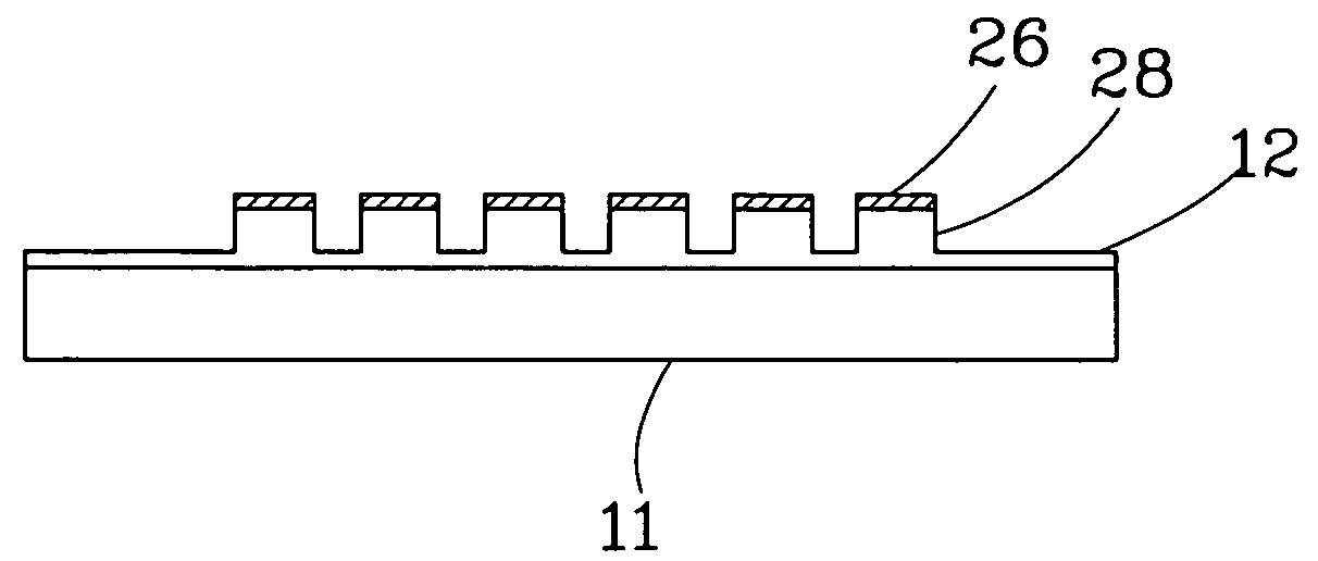
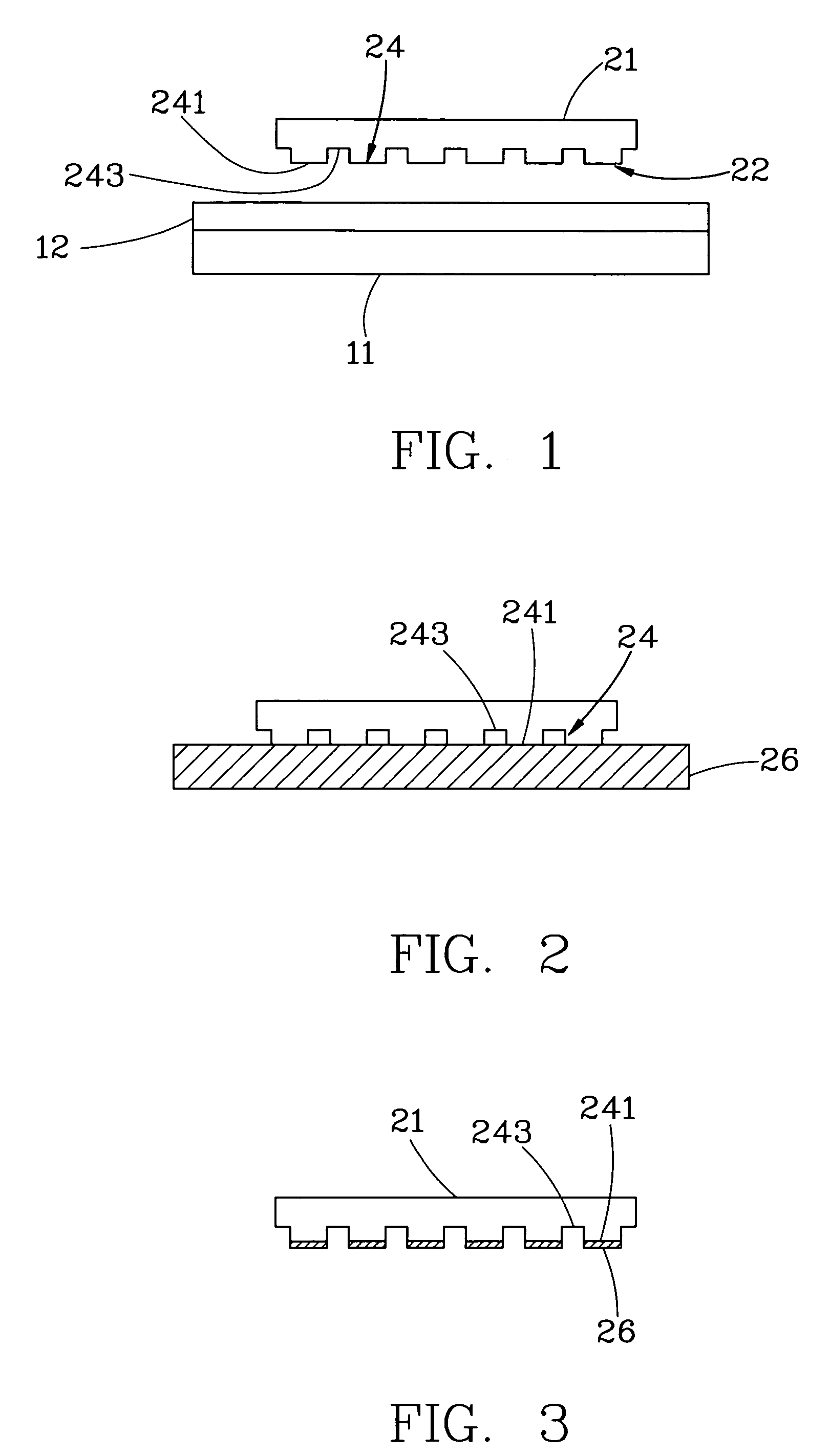
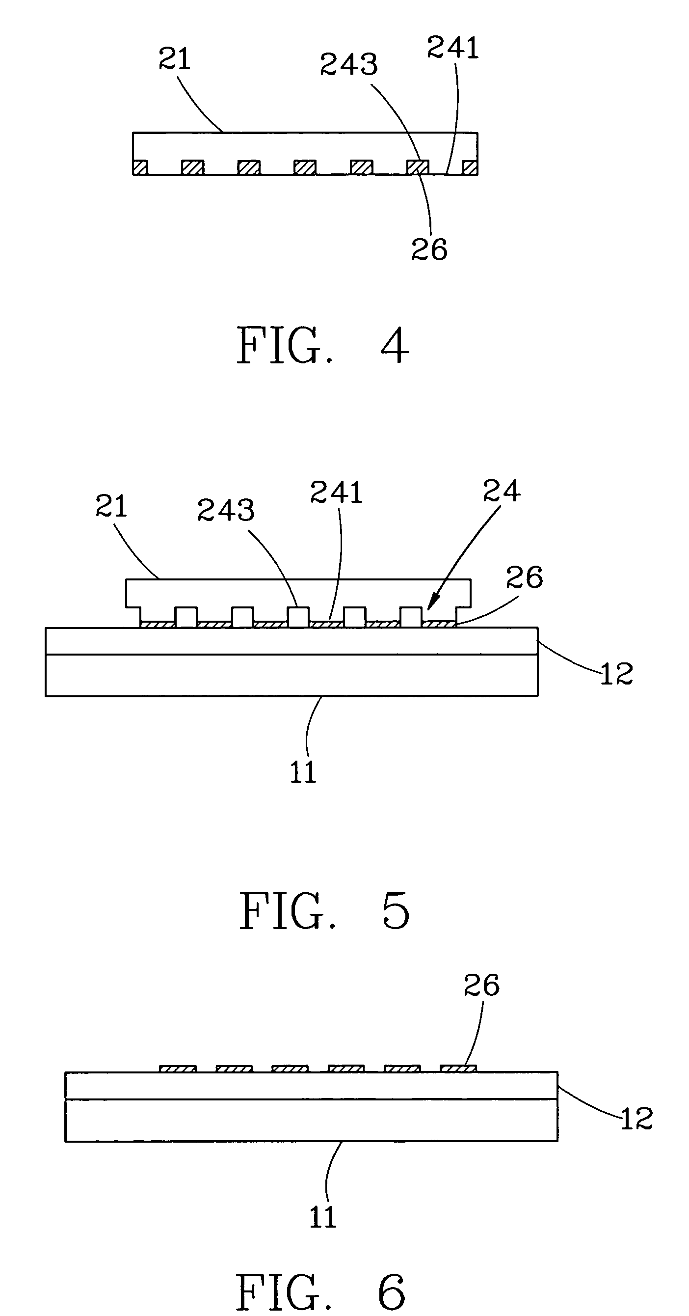
[0026] (a) Under a vacuum environment, prepare a substrate 11 and a transfer stamp 21. As shown in FIG. 1, the transfer stamp 21 is plate-like, having a transfer face 22 located on a bottom side thereof and nanometer-scale features 24 formed on the transfer face 22. The nanometer-scale features 24 are formed of a plurality of convexities 241 and concavities 243. The substrate 11 has an etched layer 12 made of polymer.

[0027] (b) Proceed a staining process, as shown in FIG. 2, to enable either the convexities 241 or the concavities 243 to be stained with a photoresist 26. FIG. 3 shows the convexities 241 stained with the photoresist 26. FIG. 4 shows the concavities 243 filled with the photoresist 26.

[0028] (c) Proceed a transfer process to enable the transfer stamp 21 to touch the substrate ...


PUM


Abstract

A nanoimprint lithography method of fabricating a nanoadhesive includes steps of (a) preparing a substrate and a transfer stamp, said transfer stamp having a transfer face and nanometer-scale features formed on said transfer face, said nanometer-scale features having a plurality of convexities and concavities, said substrate having an etched layer; (b) proceeding a staining process to enable either of said convexities and concavities to be stained with a photoresist; (c) proceeding a transfer process to enable said nanometer-scale features to touch said etched layer to transfer said photoresist onto said etched layer; and (d) proceeding an etching process to enable parts of said etched layer that are not stained with the photoresist to be each etched for a predetermined depth. As the steps indicated above, the nanoadhesive can be produced with mass production and low cost.

Description

BACKGROUND OF THE INVENTION [0001] 1. Field of the Invention [0002] The present invention relates generally to nanotechnology, and more particularly, to low-cost and high-throughput nanoimprint lithography method of fabricating a nanoadhesive. [0003] 2. Description of the Related Art [0004] In the field of the nanotechnology, the imprint lithography techniques can meet the requirements of mass production and low production cost. Particularly, the imprint lithography technique with the sub-50-nm line-width is essential for the further manufacturing of semiconductor integrated circuits and the commercialization of electronic, optoelectronic, and magnetic nanodevices. [0005] Numerous relevant technologies are under development, like scanning electron beam lithography (K. C. Beard, T. Qi. M. R. Dawson, B. Wang. C. Li, Nature 368, 604 (1994)), x-ray lithography (M. Godinot and M. Mahboubi, C. R. Acad. Sci. Ser. II Mec. Phys. Chim. Chim. Sci. Terre Univers. 319, 357(1994); M. Godinot, in ...

Claims


Application Information

Patent Timeline
IPC IPC(8): B29C43/02
CPCB29C43/003B29C43/021B29C43/06G03F7/0002B29C2043/463B82Y10/00B82Y40/00B29C2043/025B41M1/24B41M5/00
Inventor CHAO, CHIH-YUHSIEH, WEN-JIUNN
Owner CONTREL TECH CO LTD
Why Eureka
Try Eureka