

Switch, semiconductor device, and manufacturing method thereof
a technology of semiconductor devices and switches, applied in the direction of contacts, microstructured systems, relays, etc., can solve problems such as difficulty in attending, and achieve the effect of high reliability
- Summary
- Abstract
- Description
- Claims
- Application Information
AI Technical Summary
Benefits of technology
Problems solved by technology
Method used
Image

Examples
first embodiment
(First Embodiment)
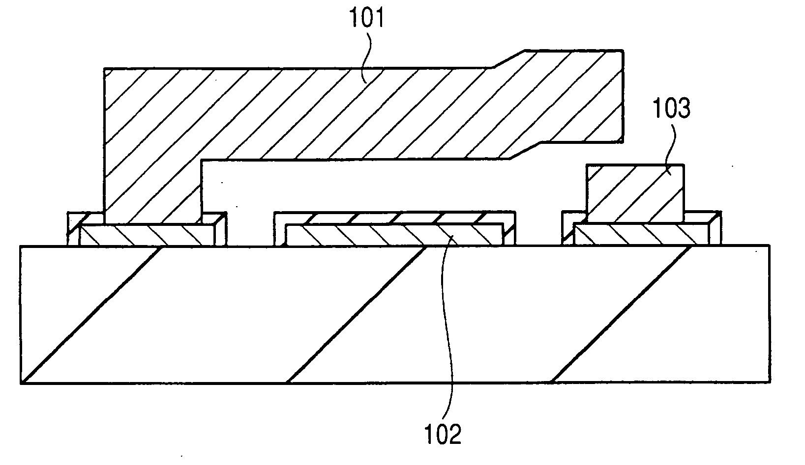
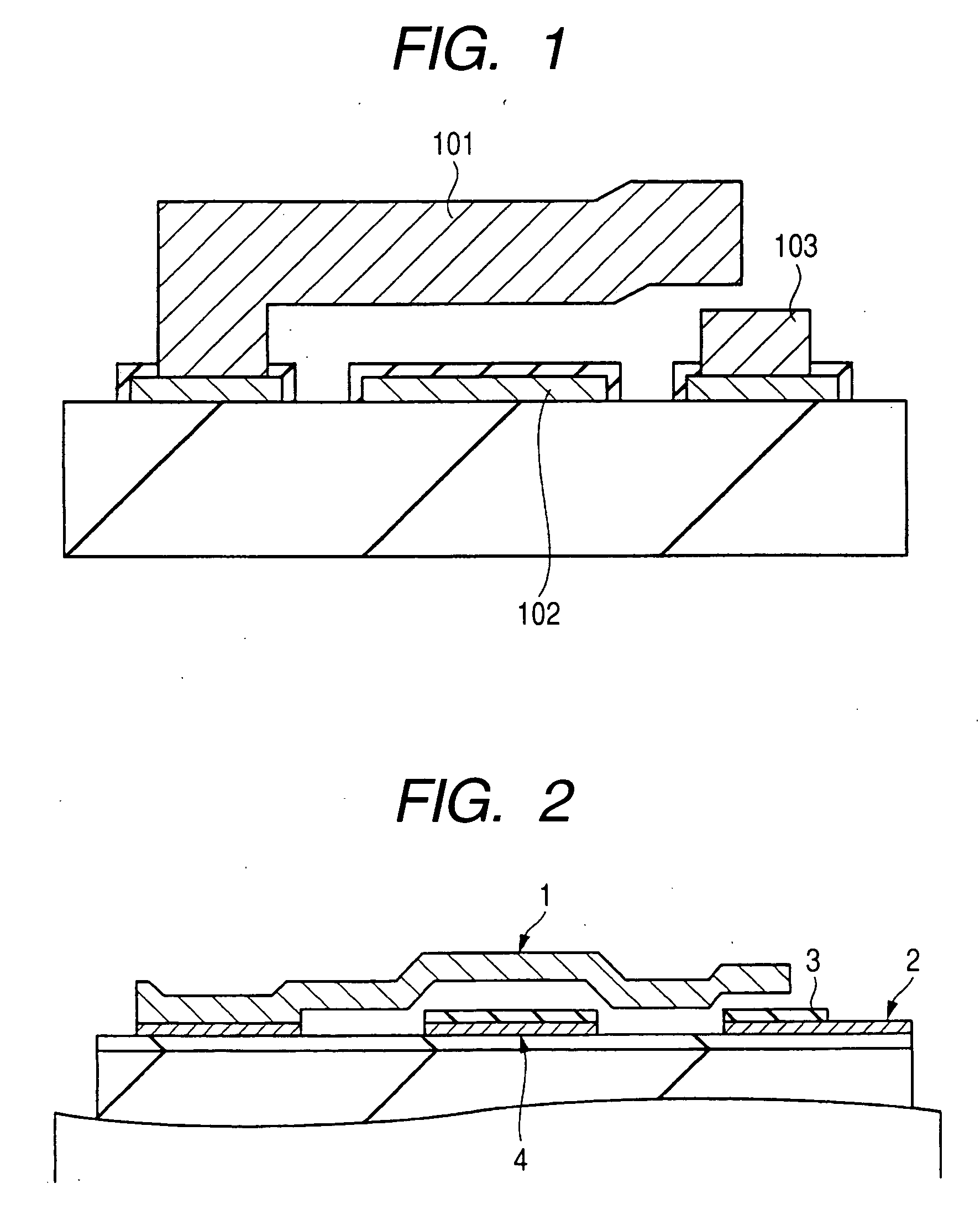
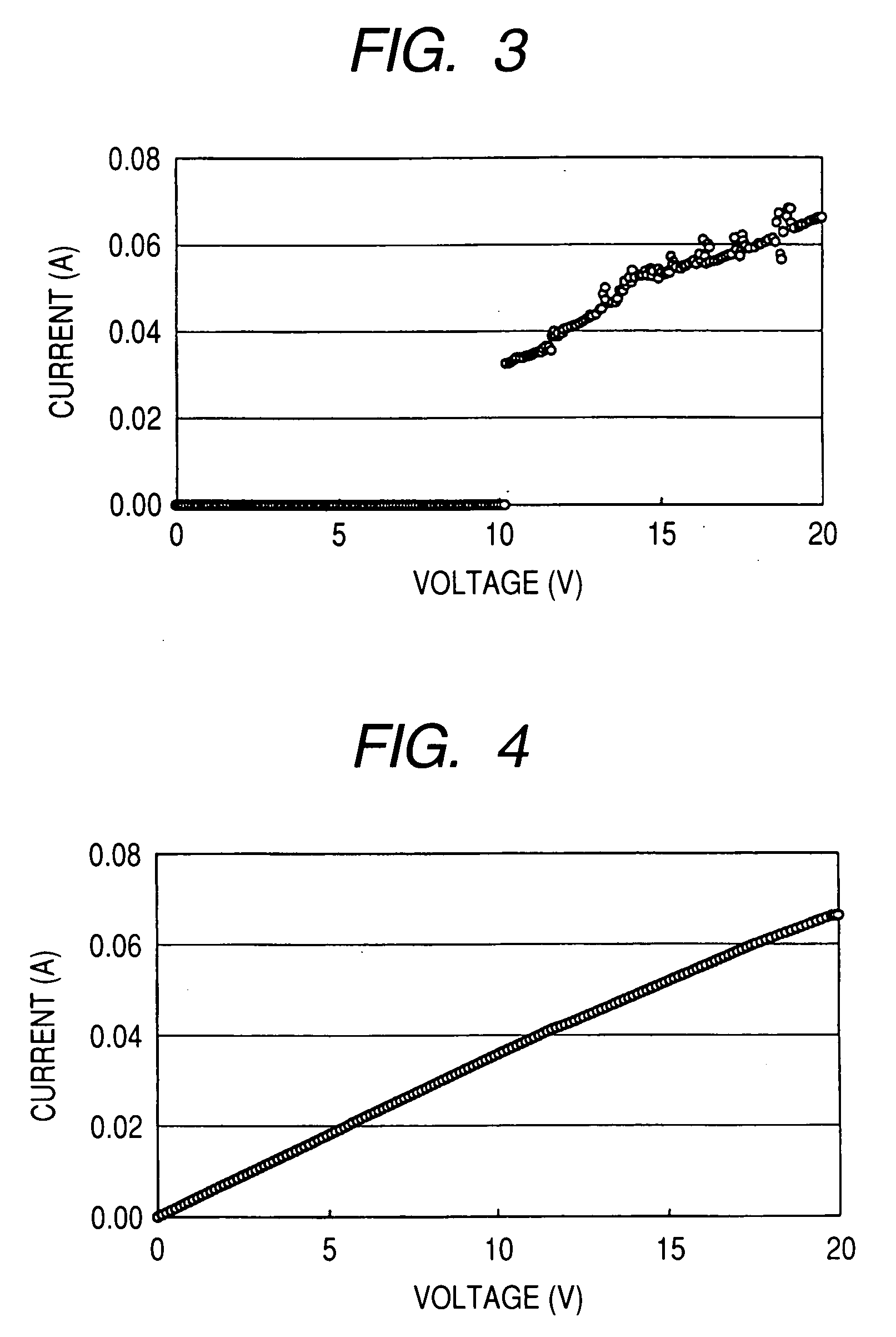
[0062] As shown in FIG. 2, the first embodiment describes a configuration consisted of an insulator 3 formed on the contact surface of a cantilever beam 1 constituting the MEMS switch and a fixed contact 2 opposite thereto. When the switch is used, the cantilever beam 1 is moved to contact the fixed contact 2 by applying a predetermined voltage between the cantilever beam 1 and a pull-in electrode 4, and a voltage exceeding the breakdown field strength of the insulator 3 is applied to the insulator 3, resulting in dielectric breakdown taking place. As mentioned above, by modifying the insulator 3 once, a contact point is achieved in which the contact point part of the switch which repeatedly makes contact is mechanically protected and the electrical signals are transmitted through the current path formed by the dialectic breakdown.
[0063] Conventionally, contact between the cantilever beam 1 and the fixed contact 2 constituting a switch has taken place by using a m...
second embodiment
(Second Embodiment)
[0116]FIG. 38 is an example in which a MEMS switch explained in the aforementioned first embodiment is used as a feeding switch for a circuit block. In FIG. 38, the mth circuit block and the nth circuit block are shown among a plurality of circuit blocks.
[0117] When the power supply of the circuit block m is ON, VINm is applied to the MEMS switch 70 to turn on the mth MEMS switch 70. The voltage of the feed line 72 is supplied to the circuit block m through the current path of this MEMS switch 70.
[0118] When the power supply of the circuit block n is ON, VINn is applied to the MEMS switch 71 to turn on the nth MEMS switch 71. The voltage of the feed line 72 is supplied to the circuit block n through the current path of this MEMS switch 71.
[0119] When VINm and VINn are simultaneously applied and the mth MEMS switch 70 and the nth MEMS switch 71 are simultaneously turned on, the circuit block m and the circuit block n can be fed at the same time. Moreover, energy...
PUM
 Abstract
Description
Claims
Application Information