
Dual BGA alloy structure for improved board-level reliability performance

a technology of alloy structure and reliability, applied in the field of semiconductor devices, can solve the problems of increasing processing time and complexity, affecting the reliability of bga packages in blr testing, and presenting challenges in finding suitable underfill materials, so as to improve the performance of bga packages, improve performance, and improve the effect of performan

Inactive Publication Date: 2007-02-01
TEXAS INSTR INC
View PDF12 Cites 26 Cited by
  • Summary
  • Abstract
  • Description
  • Claims
  • Application Information

AI Technical Summary

Benefits of technology

[0010] One of the inventors' concepts relates to a method of improving the performance of a ball grid array package under temperature cycling and drop tests. The method comprises forming a ball grid array having two types of solder balls. The first type of ball has a composition that improves performance under temperature cycling and the second set of solder balls has a composition that improves performance under drop testing. Preferably, the first set of balls is under the die near its perimeter, where temperature cycle test failures have been found to occur most frequently. Preferably, the second set of balls is located near the perimeter of the package, particularly at corners, where the majority of drop test failure have been observed. In one embodiment, the composition and properties are varied primarily through silver content, the first set of balls preferably having little or no silver and the second set of balls having a silver content in the neighborhood of 2.5%. Preferably, both sets of balls can be reflowed at one temperature.

Problems solved by technology

A common point of failure for BGA packages in BLR testing is the solder ball connections.
Adding underfill after the BGA package is attached to the PCB adds significantly to processing time and complexity, as well as cost.
Adding the material before soldering adds less complexity, but presents challenges in finding suitable underfill materials that are compatible with solders.

Method used


Image

  • Dual BGA alloy structure for improved board-level reliability performance
  • Dual BGA alloy structure for improved board-level reliability performance

Examples


Embodiment Construction

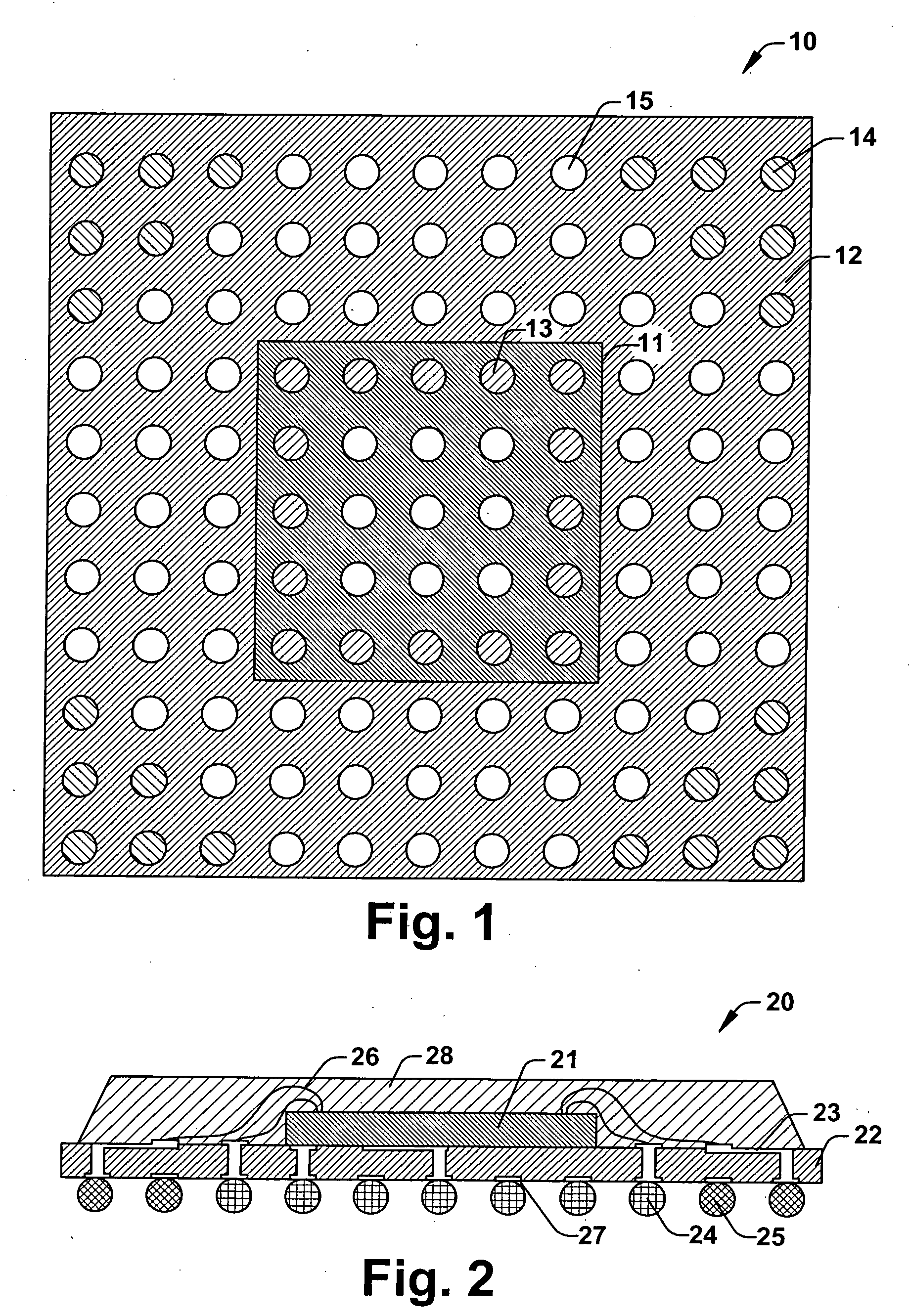
[0016] BLR temperature cycle and drop testing were carried out for PCB mounted BGA packages attached with Sn—Ag—Cu alloy solder balls. When failures occurred, the locations of the failures typically depended on the test. FIG. 1 illustrates the failure pattern for a BGA package 10 comprising a die 11 mounted on a substrate 12. When a drop test failure occurred, the failure was typically at the package corner in the area indicated by the solder balls 14. When a temperature cycle test failure occurred, it was typically at a location under the die near the die edge in the area indicated by the solder balls 13. The remaining solder balls 15 typically do not fail.

[0017] Further studies indicated that either drop test failures or temperature cycle test failures could be eliminated by varying the silver content of the solder. Starting from Sn1.2Ag0.5Cu (1.2% Ag and 0.5% Cu, balance Sn), tests were conducted with varying silver content. Drop test failures decreased with silver content, the ...


PUM


Abstract

A method of improving the performance of a ball grid array package under temperature cycling and drop tests is disclosed. The method comprises forming a ball grid array with two types of solder balls. The first type of ball has a composition that improves performance under temperature cycling and the second set of solder balls has a composition that improves performance under drop testing. Preferably, the first set of balls is under the die near its perimeter and the second set of balls is located near the package perimeter, particularly at corners. A related concept pertains to a semiconductor device comprising a printed circuit board and a ball grid array package attached to the printed circuit board by an array of solder balls. The solder ball array comprises first and second sets of solder balls, the two sets having distinctly different compositions.

Description

FIELD OF THE INVENTION [0001] The present invention relates generally to semi-conductor devices and more specifically to Ball Grid Array (BGA) packages. BACKGROUND OF THE INVENTION [0002] Maximizing reliability, lowering cost and increasing feature density to improve performance are ongoing goals of semi-conductor device manufacturers. In particular, the demands of portable systems, such as computers and telecommunications, have spurred efforts to create reliable technology for supplying circuits having the smallest possible area and highest possible operating speed. [0003] Semi-conductor device manufacturing typically begins with semi-conductor wafers. Various features are patterned on and into the wafers. The wafers are then singulated to form dies. To facilitate the attachment of these dies to printed circuit boards (PCBs) and to protect the dies, which are relatively fragile, the dies are typically assembled into packages before they are interconnected with PCBs. In addition to ...

Claims


Application Information

Patent Timeline
Patent Type & Authority Applications(United States)
IPC IPC(8): H01L23/48
CPCH01L23/49816H01L23/49866H01L24/48H01L2224/48227H01L2924/01322H01L2924/15311H01L2924/00H01L2924/181H01L2924/00014H01L2924/00012H01L2224/45099H01L2224/45015H01L2924/207
Inventor BEDDINGFIELD, STANLEY CRAIG
Owner TEXAS INSTR INC
Learn More