Nonvolatile semiconductor memory device and a method for programming nand type flash memory

a nonvolatile semiconductor and memory device technology, applied in static storage, digital storage, instruments, etc., can solve the problems of gidl not being thoroughly prevented, program errors easily occurring, and channel potential being overly raised, so as to suppress gidl, suppress program errors, and high reliability

Active Publication Date: 2007-02-01
KIOXIA CORP
View PDF7 Cites 25 Cited by
  • Summary
  • Abstract
  • Description
  • Claims
  • Application Information

AI Technical Summary

Benefits of technology

[0018] Accordingly, this invention deals with the above mentioned problems and attempts to provide a highly reliable non-volatile semiconductor memory device, such as NAND type flash memory, to suppress GIDL which usually occurs during “1” data programming and to suppress program errors without making great changes to flash memory device structures.

Problems solved by technology

However, the potential of the channel could be overly raised from the floating state.
As a result, program errors can easily occur.
In the conventional method, however, GIDL may not be thoroughly prevented; especially when “1” data programming, leading to program errors and a deterioration in the reliability of the NAND type flash memory.
On the other hand, the disadvantage of the EASB method is that a coupling ratio of the floating gate of the programming memory cells becomes lower when “0” programming is performed, because a potential of the word lines adjacent to the source line side from the selected word line is Vss.
However, there is a disadvantage in both the EASB method and EASB-2 method, that the closer the selected word lines to the bit line, the higher the boost effect becomes in the memory cells on the bit line side, than in the program memory cells, and thus the potential of the memory cell channels become too high.
However it is difficult to suppress the GIDL to a sufficient level.

Method used


Image

  • Nonvolatile semiconductor memory device and a method for programming nand type flash memory
  • Nonvolatile semiconductor memory device and a method for programming nand type flash memory
  • Nonvolatile semiconductor memory device and a method for programming nand type flash memory

Examples


first embodiment

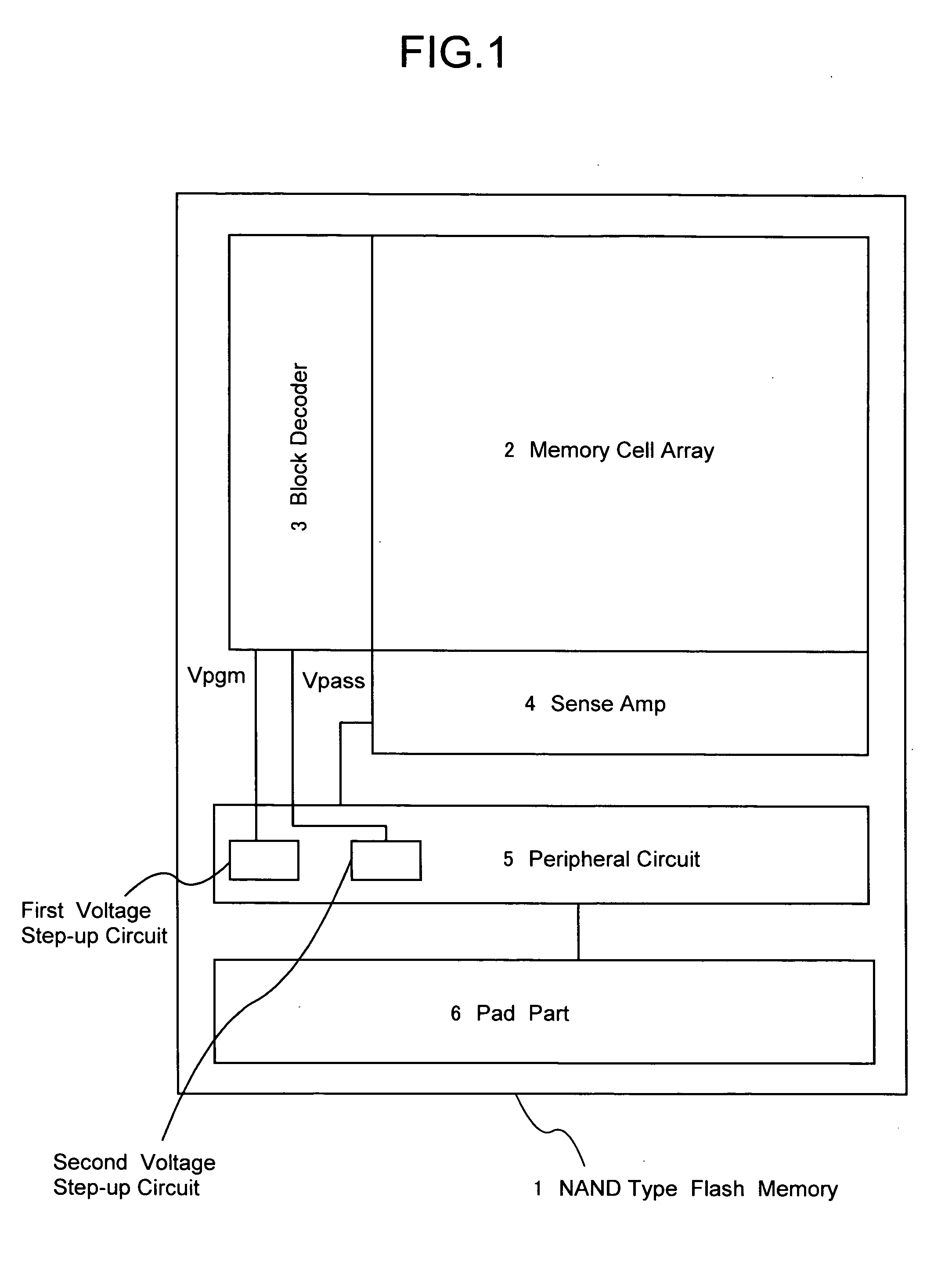
[0038]FIG. 1 shows a schematic block diagram of a NAND type flash memory according to one embodiment for a nonvolatile semiconductor memory device of the present invention. NAND type flash memory 1 shown in FIG. 1 comprises a memory cell array 2 in which a plurality of electrically programmable memory cells are arranged in matrix, a block decoder 3, a sense amplifier 4, a peripheral circuit 5, and a pad part.

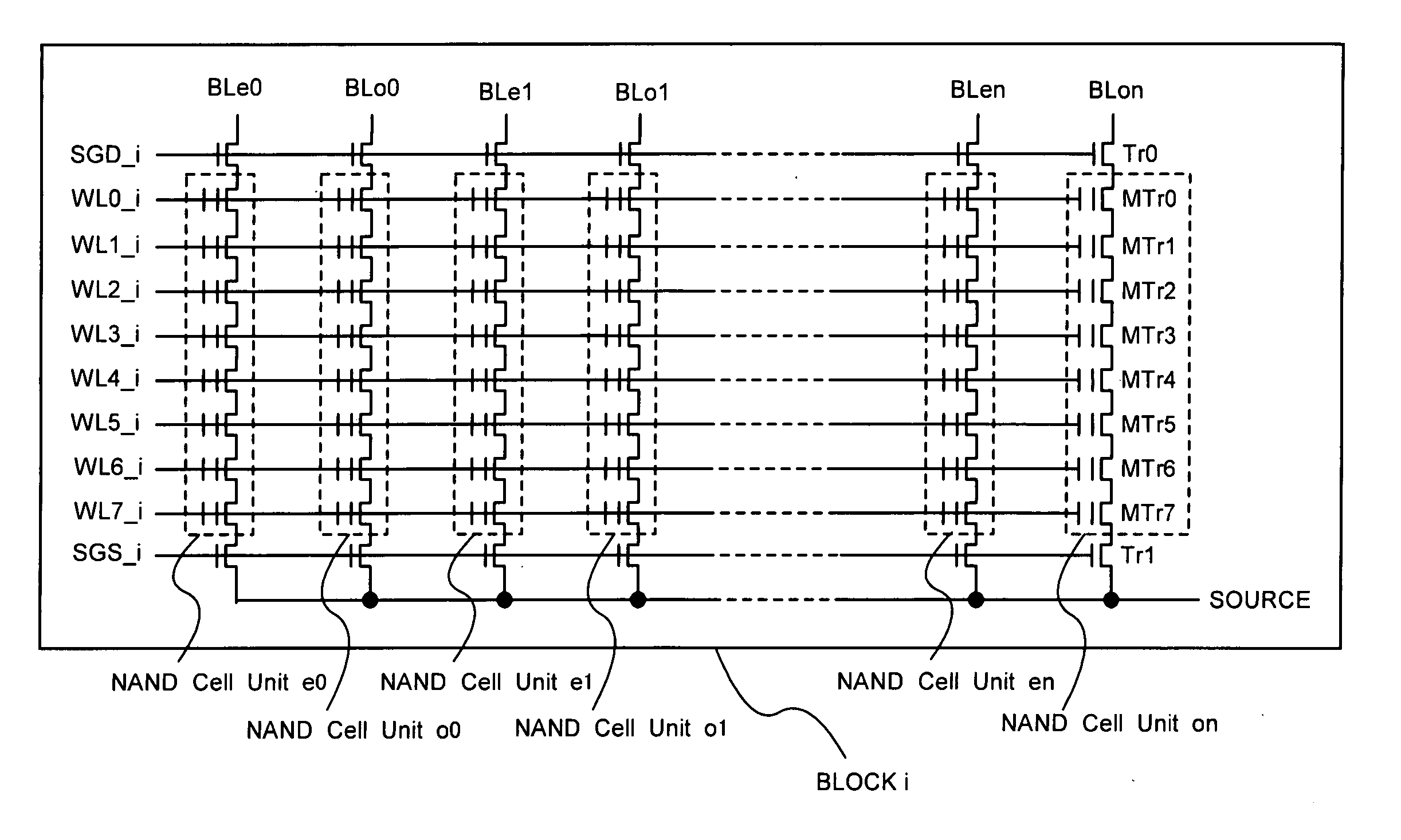
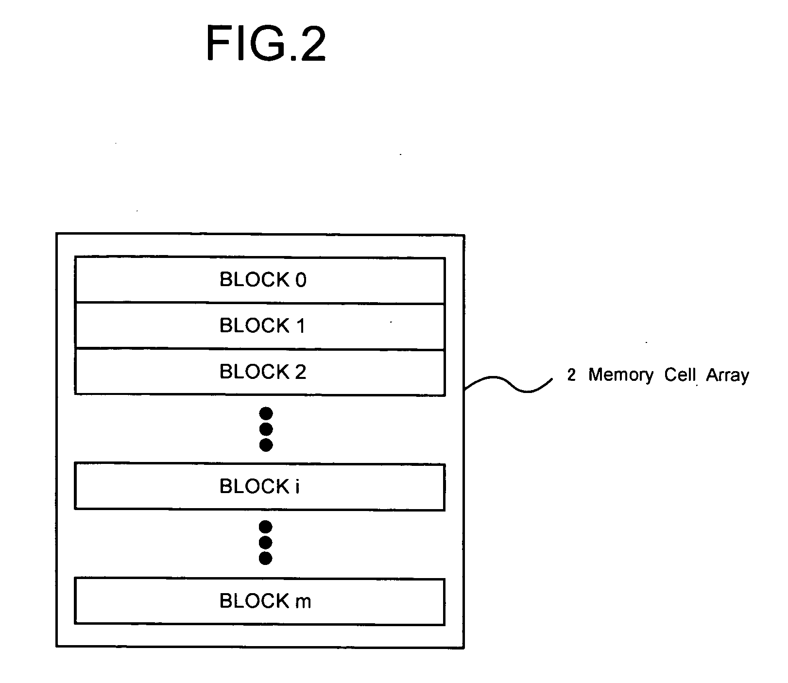
[0039]FIG. 2 shows a configuration of the memory cell array 2. As shown in FIG. 2, the memory cell array 2 is divided into total m blocks (BLOCK 0, BLOCK 1, . . . , BLOCKi, . . . , BLOCK m). “Block” is a minimum unit for a data erasure.

[0040] Each of the blocks BLOCK 0 to BLOCK m is configured with 2n NAND cell units e 0 to en, as FIG. 3 shows representative BLOCKi. In this embodiment, each of the NAND cell units is configured with series-connected 8 memory cells MTr0 to MTr7. The one end is connected to the bit line (BLe0, BL o0, ..., BL en to BL on) via selection gate transi...

second embodiment

[0055] In the present embodiment, another driving method of the NAND type flash memory according to the embodiment of the nonvolatile semiconductor memory devices in the present invention will be explained.

[0056] In this embodiment, the configuration is not explained because the configuration is the same as the NAND type flash memory 1 of the above-mentioned embodiment, except for a driving method during programming.

[0057] Referring to FIG. 5, a data programming operation of a NAND type flash memory 1 of the present invention will be explained. The program operation of the embodiment is the SB method. In FIG. 5, as explained in the above-mentioned embodiment, changes for set potentials of each of the word lines WL0 to WL7 are shown, in the case where the memory cells are connected to word line WL2 in the selected NAND cell unit in which, for example, even number pages of the BLOCKi is selected for programming (for example, NAND cell unit e0 of the BLOCKi), in the data programming ...

third embodiment

[0072] In the present embodiment, another driving method of the NAND type flash memory according to the embodiment of the nonvolatile semiconductor memory devices in the present invention will be explained.

[0073] In this embodiment, the configuration is not explained because the configuration is the same as the NAND type flash memory 1 of the above-mentioned embodiment, except for a driving method during programming.

[0074] Referring to FIG. 6, a data programming operation of a NAND type flash memory 1 of the present invention will be explained. The program operation of this embodiment is ONE variation of SB 2 method. In FIG. 6, as well as the above-mentioned embodiment, changes for set potentials of each of the word lines WL0 to WL7 are shown, in the case where the memory cells connected to word line WL2 in the selected NAND cell unit in which, for example, even number pages of the BLOCKi is selected for a data programming (for example, NAND cell unit e0 of the BLOCKi), in the dat...


PUM


Abstract

A non-volatile semiconductor memory device comprise a memory cell array having a plurality of memory cell units each having a plurality of electrically-programmable memory cell connected in series, a plurality of word lines each connected to each of control gates of said plurality of memory cells, said plurality of word lines including a selected word line connected to a control gate of selected one of said memory cells for programming, and a plurality of unselected word lines different from said selected word line, a bit line connected to one end of said memory cell unit, and a source line connected to another end of the memory cell unit, wherein, when data is programmed into the selected memory cells, a first potential is supplied to said selected word line, and a first unselected word line adjacent, toward a source line side, to said selected word line is set to floating state, and thereafter, a second potential which is higher than said first potential is supplied to said selected word line.

Description

CROSS-REFERENCE TO RELATED APPLICATIONS [0001] This application is based upon and claims the benefit of priority from the prior Japanese Patent Application No. 2005-222698, filed on Aug. 1, 2005, the entire contents of which are incorporated herein by reference. TECHNICAL FIELD [0002] The present invention relates to an electrically programmable nonvolatile semiconductor memory device and its programming method, and more particularly to a method for data programming NAND type flash memory. BACKGROUND OF THE INVENTION [0003] Recently, demand for nonvolatile semiconductor memory devices which are compact and have large capacity have been increasing rapidly. Among these, a NAND type flash memory, in which higher integration and larger capacity are expected as compared with a conventional NOR type flash memory, has attracted attention. [0004] In the program operation of a conventional NAND type flash memory, Self Boost Method (SB) is used, wherein NAND cell units including memory cells ...

Claims


Application Information

Patent Timeline
Patent Type & Authority Applications(United States)
IPC IPC(8): G11C11/34
CPCG11C16/0483G11C16/3427G11C16/3418G11C16/10
Inventor FUTATSUYAMA, TAKUYA
Owner KIOXIA CORP
Why Eureka
Try Eureka