

Vapor phase deposition apparatus and vapor phase deposition method
a technology of vapor phase and deposition apparatus, which is applied in the direction of chemically reactive gases, crystal growth process, coatings, etc., can solve the problem of broken silicon wafer b>200/b>
- Summary
- Abstract
- Description
- Claims
- Application Information
AI Technical Summary
Benefits of technology
Problems solved by technology
Method used
Image

Examples
first embodiment
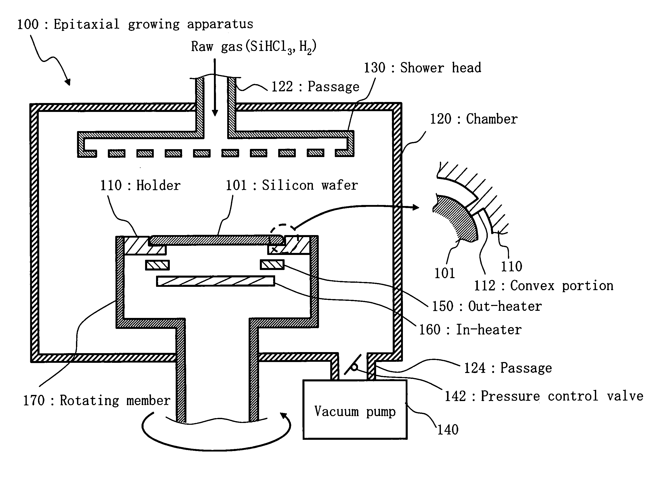
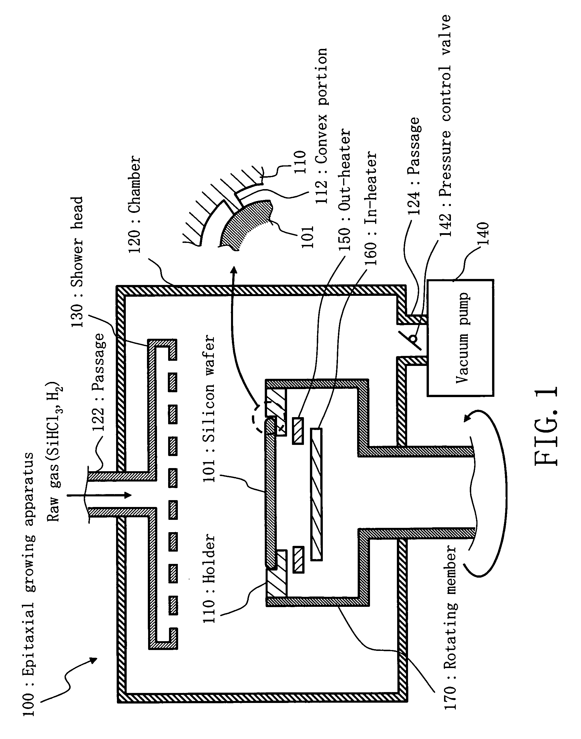
[0049]FIG. 1 is a conceptual view showing a structure of an epitaxial deposition apparatus according to a first embodiment.
[0050] In FIG. 1, an epitaxial deposition apparatus 100 according to an example of a vapor phase deposition apparatus or “device” includes a holder (which may also be referred to herein as a susceptor) 110 as to an example of a support table, a chamber 120, a shower head 130, a vacuum pump 140, a pressure control valve 142, an out-heater 150, an in-heater 160 and a rotating member 170. A passage 122 which supplies a gas and a passage 124 which discharges the gas are connected to the chamber 120. The passage 122 is connected to the shower head 130. In FIG. 1, necessary structures for explaining the first embodiment are illustrated. The epitaxial deposition apparatus 100 may be provided with portions other than structures in FIG. 1. Moreover, a contraction scale or the like is not coincident with a real object (This applies to other drawings also).
[0051] The hol...
second embodiment
[0092] While the first projecting portion is provided to reduce the contact region of the film grown in the side surface portion of the substrate and the film deposited on the holder side in the first embodiment, description will be given to the shape of the holder in which advantages are poor but the contact region is reduced more greatly than that in the conventional art in a second embodiment.
[0093]FIG. 22 is a top view showing an example of a state in which a silicon wafer is supported on a holder according to the second embodiment.
[0094]FIG. 23 is a sectional view showing a section of the state in which the silicon wafer is supported on the holder illustrated in FIG. 22.
[0095] A counterbore or depressed portion having a diameter larger than a diameter of a silicon wafer 101 is formed on a holder 110, and a ring 118 having a circular section is disposed in the counterbore. In other words, the holder 110 includes the ring 118 in which a surface to constrain a movement in the s...
PUM
| Property | Measurement | Unit |
|---|---|---|
| Height | aaaaa | aaaaa |
| Height | aaaaa | aaaaa |
| Height | aaaaa | aaaaa |
Abstract
Description
Claims
Application Information