Methods for fabricating a stressed MOS device

a stress-strength technology, applied in the direction of semiconductor devices, basic electric elements, electrical equipment, etc., can solve the problems of reducing electron mobility, and the present techniques for increasing the mobility of carriers by embedding expanding materials cannot be applied in the same way to both p-channel and n-channel mos transistors

Inactive Publication Date: 2007-02-01
GLOBALFOUNDRIES INC
View PDF15 Cites 53 Cited by
  • Summary
  • Abstract
  • Description
  • Claims
  • Application Information

AI Technical Summary

Problems solved by technology

Such a compressive longitudinal stress, however, decreases the mobility of electrons, the majority carriers in N-channel MOS transistors.
Unfortunately, present techniques for increasing carrier mobility by embeddin

Method used


Image

  • Methods for fabricating a stressed MOS device
  • Methods for fabricating a stressed MOS device
  • Methods for fabricating a stressed MOS device

Examples


Embodiment Construction

[0009] The following detailed description is merely exemplary in nature and is not intended to limit the invention or the application and uses of the invention. Furthermore, there is no intention to be bound by any expressed or implied theory presented in the preceding technical field, background, brief summary or the following detailed description.

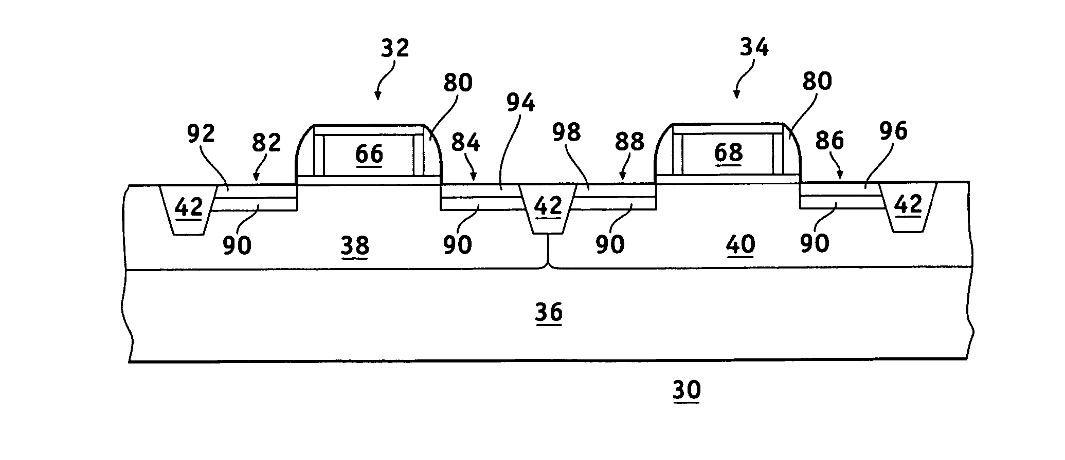
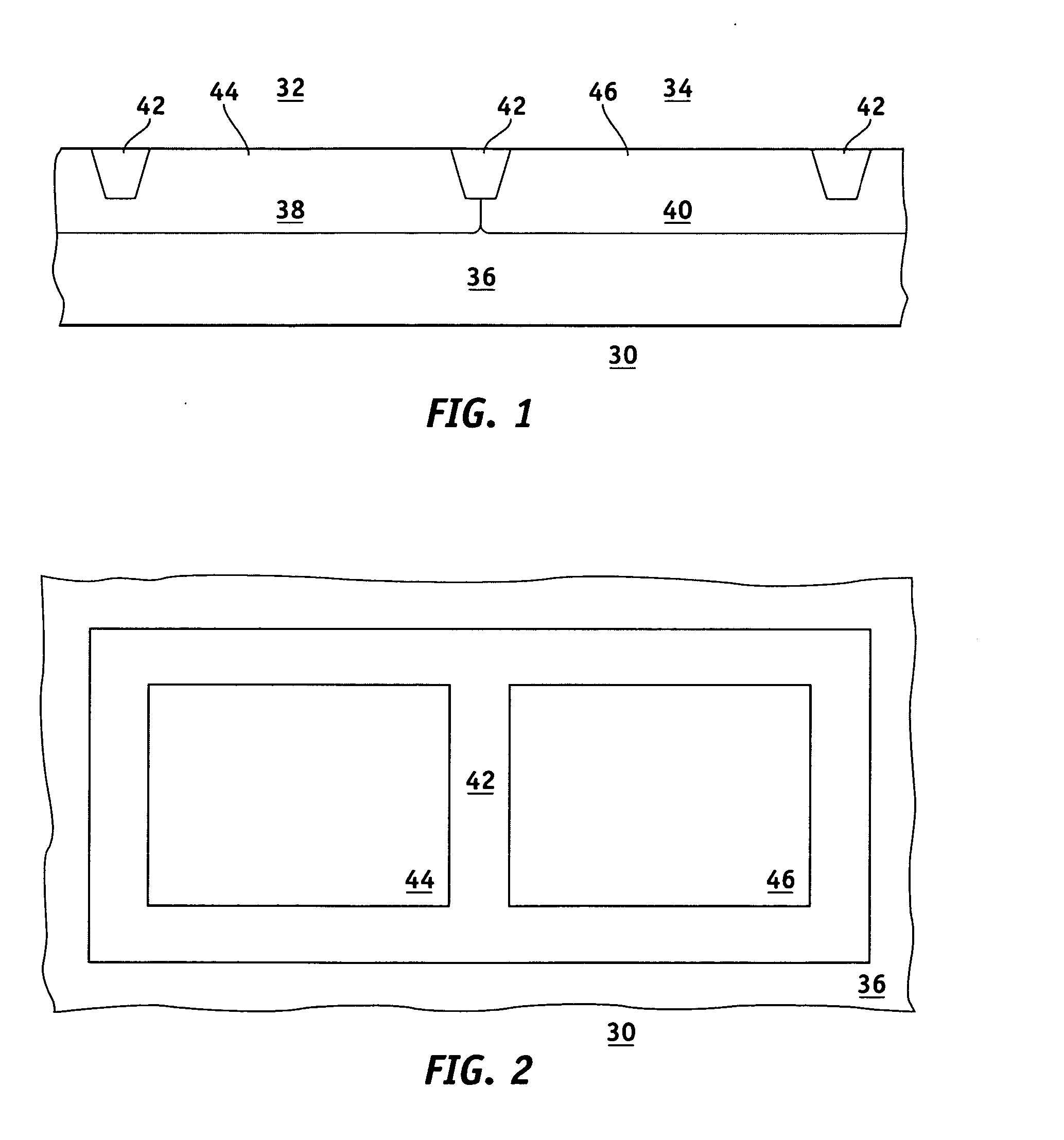
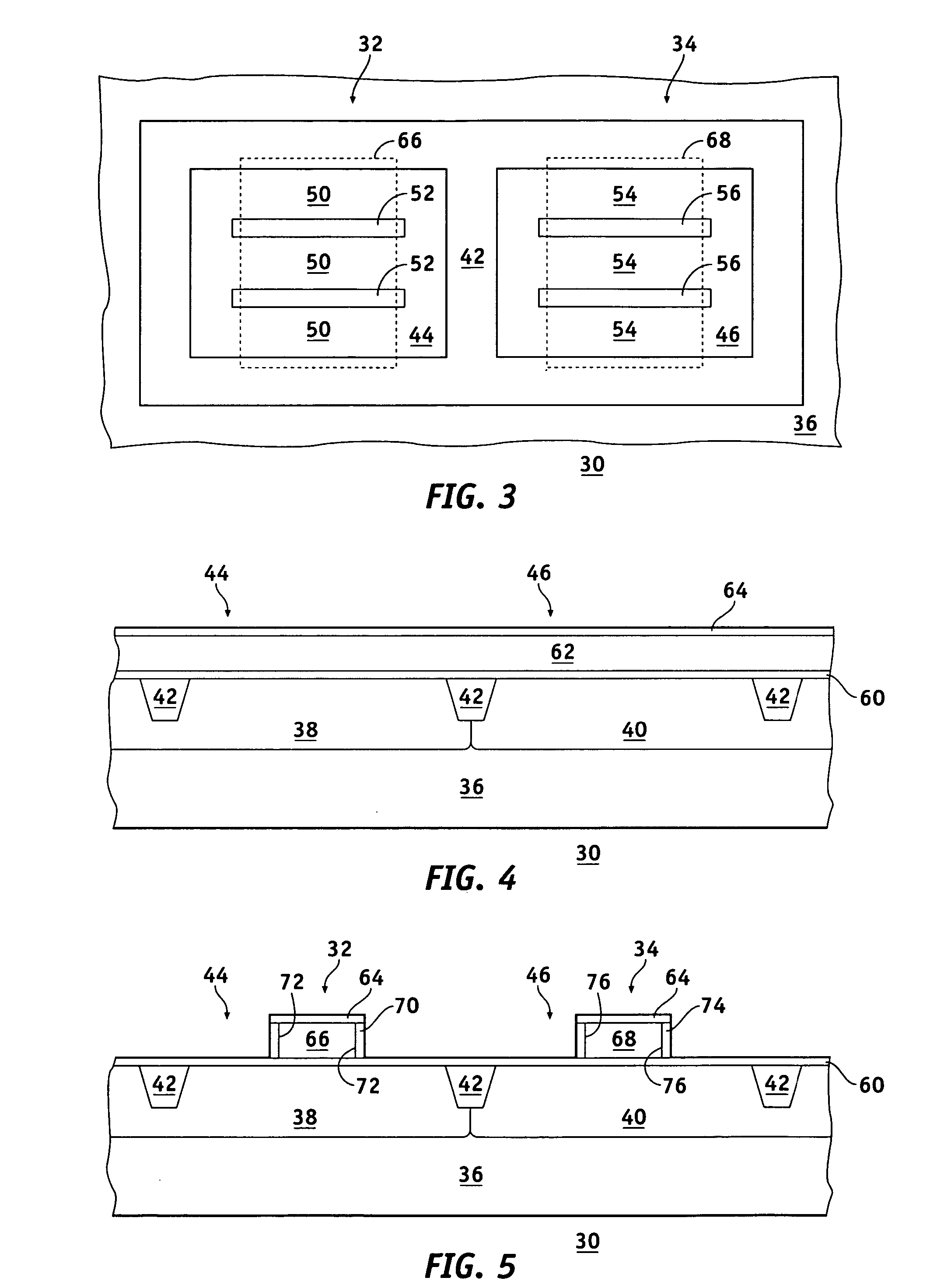
[0010] In a typical complementary MOS (CMOS) integrated circuits, high performance P-channel MOS transistors N-channel MOS transistors each have a relatively wide channel width to provide sufficient drive current. The channel width of such transistors is on the order of 1 μm while the channel length and the depth of the source and drain regions are less than about 0.1 μm. If stress inducing material having a thickness of the same order of magnitude as the source and drain regions is embedded at the ends of the channel, such stress inducing materials can apply a longitudinal stress along the channel, but are relatively ineffective in appl...


PUM


Abstract

Methods are provided for fabricating a stressed MOS device. The method comprises the steps of forming a plurality of parallel MOS transistors in and on a semiconductor substrate. The parallel MOS transistors having a common source region, a common drain region, and a common gate electrode. A first trench is etched into the substrate in the common source region and a second trench is etched into the substrate in the common drain region. A stress inducing semiconductor material that has a crystal lattice mismatched with the semiconductor substrate is selectively grown in the first and second trenches. The growth of the stress inducing material creates both compressive longitudinal and tensile transverse stresses in the MOS device channel that enhance the drive current of P-channel MOS transistors. The decrease in drive current of N-channel MOS transistors caused by the compressive stress component is offset by the tensile stress component.

Description

TECHNICAL FIELD OF THE INVENTION [0001] The present invention generally relates to methods for fabricating semiconductor devices, and more particularly relates to methods for fabricating stressed MOS devices. BACKGROUND OF THE INVENTION [0002] The majority of present day integrated circuits (ICs) are implemented by using a plurality of interconnected field effect transistors (FETs), also called metal oxide semiconductor field effect transistors (MOSFETs), or simply MOS transistors. An MOS transistor includes a gate electrode as a control electrode and spaced apart source and drain electrodes between which a current can flow. A control voltage applied to the gate electrode controls the flow of current through a channel between the source and drain electrodes. [0003] MOS transistors, in contrast to bipolar transistor, are majority carrier devices. The gain of an MOS transistor, usually defined by the transconductance (gm), is proportional to the mobility of the majority carrier in the...

Claims


Application Information

Patent Timeline
IPC IPC(8): H01L21/8238H01L29/94
CPCH01L21/823807H01L21/823814H01L21/823878H01L29/7848H01L29/66636H01L29/78H01L29/165
Inventor PEIDOUS, IGORSULTAN, AKIFPELELLA, MARIO M.
Owner GLOBALFOUNDRIES INC
Why Eureka
Try Eureka