Reduced crosstalk CMOS image sensors

Active Publication Date: 2007-02-08
APTINA IMAGING CORP
View PDF5 Cites 18 Cited by
  • Summary
  • Abstract
  • Description
  • Claims
  • Application Information

AI Technical Summary

Benefits of technology

[0003] A CMOS image sensor having high sensitivity and low crosstalk, particularly at farred to infrared wavelengths, and a method for fabricating a CMOS image sensor. A CMOS image sensor in accordance with the invention has a substrate, an epitaxial layer above the substrate, and a plurality of pixels extending into the epitaxial layer for receiving light. The

Problems solved by technology

CMOS (Complementary Metal-Oxide Semiconductor) image sensors suffer from both reduced sensitivity and increased crosstalk in the far-red to infrared wavelength range (from about 700 nm to about 1 mm) because the absorption depth at these wavelengths is much larger than the pixel depth.
The diffusion length in the l

Method used


Image

  • Reduced crosstalk CMOS image sensors
  • Reduced crosstalk CMOS image sensors
  • Reduced crosstalk CMOS image sensors

Examples


Embodiment Construction

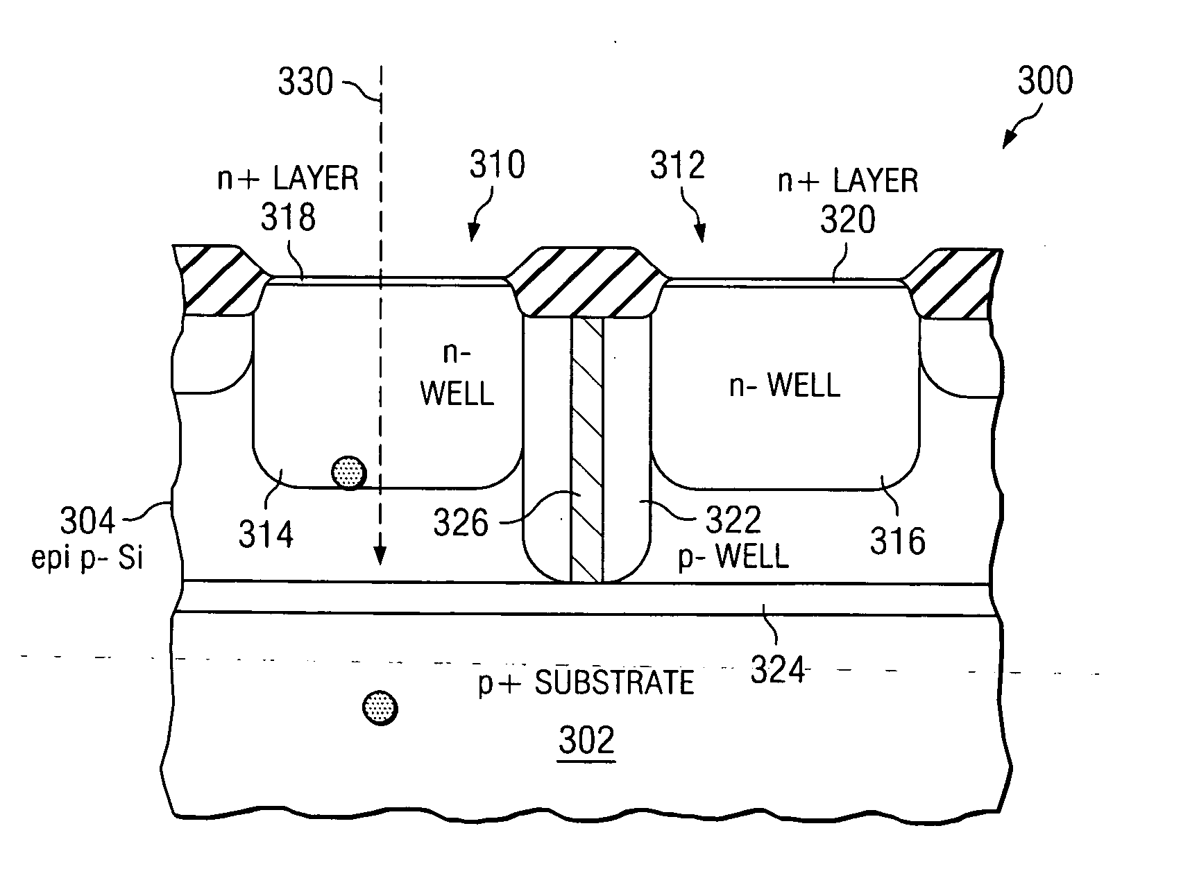
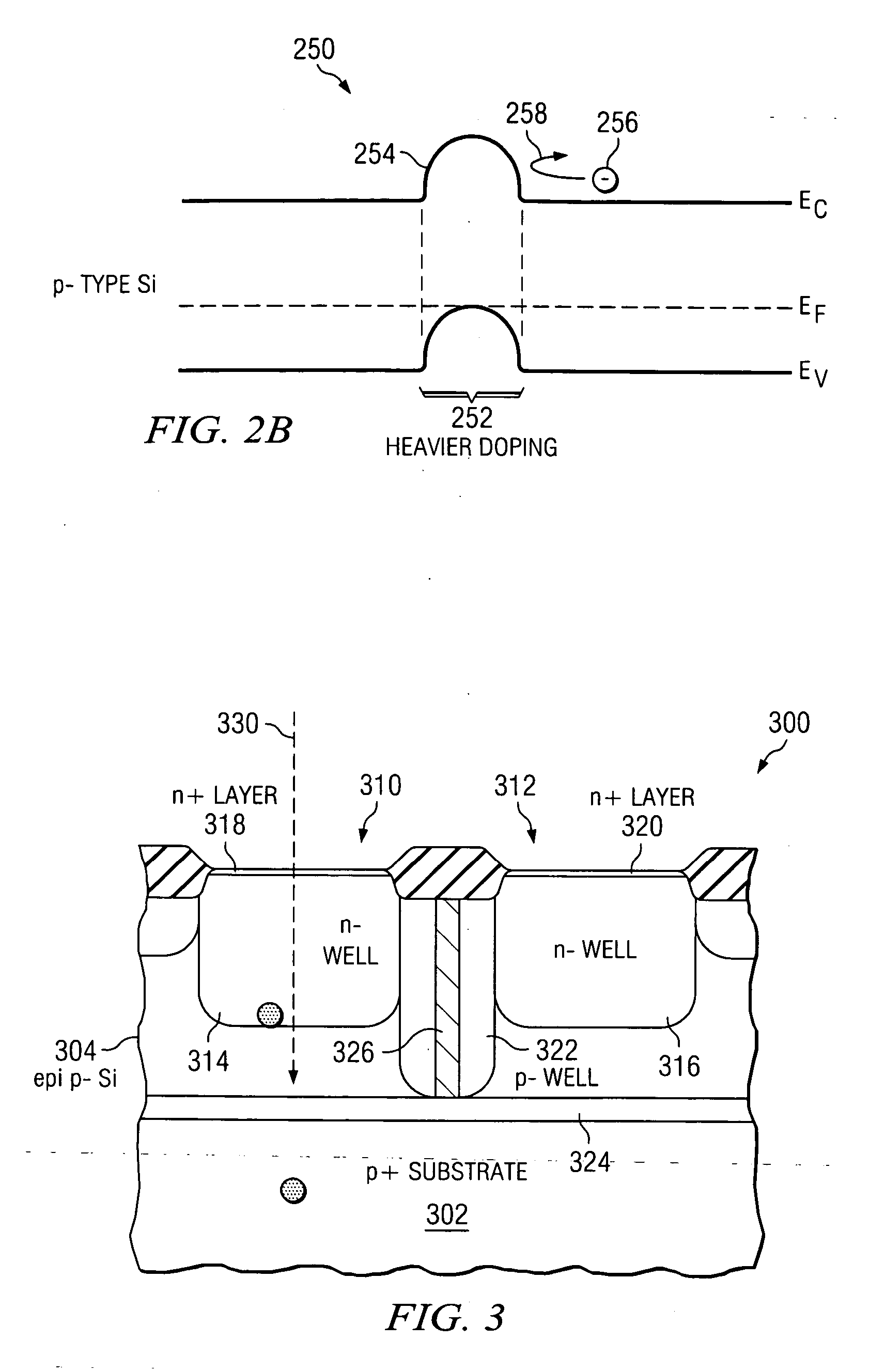
[0012] Exemplary embodiments in accordance with the invention provide a CMOS image sensor that has high sensitivity and low crosstalk, particularly at far-red to infrared wavelengths, and to a method for fabricating a CMOS image sensor.

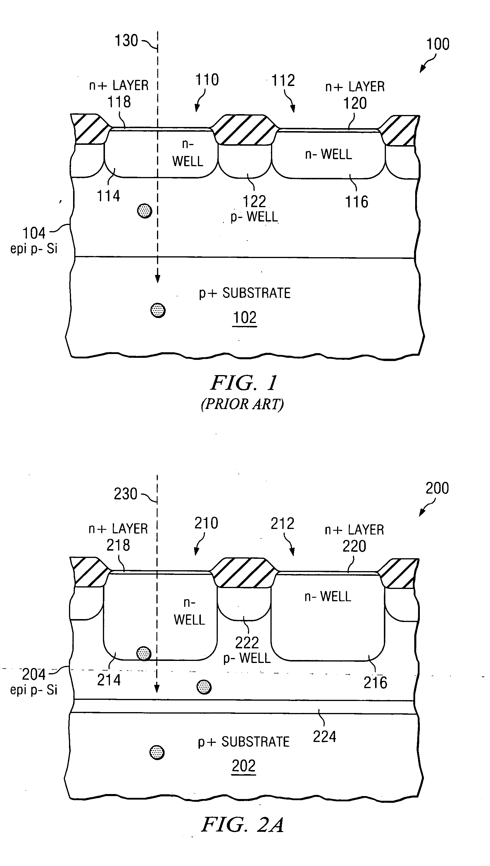
[0013]FIG. 1 is a schematic cross-sectional side view of a portion of a CMOS image sensor that is known in the art to assist in explaining the present invention. The CMOS image sensor is designated by reference number 100 and generally includes substrate 102, epitaxial (epi) layer 104 above substrate 102 and a plurality of pixels (only two pixels 110 and 112 are illustrated in FIG. 1) arranged in an array and extending into epi layer 104. Substrate 102 and epi layer 104 are both composed of silicon semiconductor material; however, substrate 102 is made of P+ (highly doped P-type) semiconductor material), and epi layer 104 is made of P− (lightly doped P-type) semiconductor material.

[0014] Pixels 110 and 112 include photodiode n-wells 114 and 116, res...


PUM


Abstract

CMOS image sensor having high sensitivity and low crosstalk, particularly at far-red to infrared wavelengths, and a method for fabricating a CMOS image sensor. A CMOS image sensor has a substrate, an epitaxial layer above the substrate, and a plurality of pixels extending into the epitaxial layer for receiving light. The image sensor also includes at least one of a horizontal barrier layer between the substrate and the epitaxial layer for preventing carriers generated in the substrate from moving to the epitaxial layer, and a plurality of lateral barrier layers between adjacent ones of the plurality of pixels for preventing lateral diffusion of electrons in the epitaxial layer.

Description

DESCRIPTION OF RELATED ART [0001] CMOS (Complementary Metal-Oxide Semiconductor) image sensors suffer from both reduced sensitivity and increased crosstalk in the far-red to infrared wavelength range (from about 700 nm to about 1 mm) because the absorption depth at these wavelengths is much larger than the pixel depth. Increased crosstalk occurs because light striking the image sensor penetrates well below the silicon surface of the sensor, and electron-hole pairs are generated deep within the substrate. These depths are well below the collection range of the pixels, and the photo-generated carriers are thus free to diffuse in all directions. The diffusion length of electrons for commonly used substrates is about 5 μm, and it is relatively easy for electrons to diffuse into adjacent pixels and cause crosstalk. The diffusion length in the lower-doped epi (epitaxial) layer can be much larger, and this can also have serious crosstalk consequences in an improperly designed image sensor....

Claims


Application Information

Patent Timeline
IPC IPC(8): H01L31/113
CPCH01L27/1463H01L27/14687H01L27/14649
Inventor BAHL, SANDEEPLAMASTER, FREDRICKBIGELOW, DAVID
Owner APTINA IMAGING CORP
Why Eureka
Try Eureka