Non-volatile memory semiconductor device having an oxide-nitride-oxide (ONO) top dielectric layer

a semiconductor device and non-volatile technology, applied in semiconductor/solid-state device manufacturing, semiconductor devices, semiconductor devices, etc., can solve the problems of negative impact on the time it takes to erase a memory cell, charge loss after many program/erase cycles, and degradation of nrom devices

a semiconductor device and non-volatile technology, applied in semiconductor/solid-state device manufacturing, semiconductor devices, semiconductor devices, etc., can solve the problems of negative impact on the time it takes to erase a memory cell, charge loss after many program/erase cycles, and degradation of nrom devices

US20070029625A1Active Publication Date: 2007-02-08MACRONIX INT CO LTD

Image

  • Non-volatile memory semiconductor device having an oxide-nitride-oxide (ONO) top dielectric layer
  • Non-volatile memory semiconductor device having an oxide-nitride-oxide (ONO) top dielectric layer
  • Non-volatile memory semiconductor device having an oxide-nitride-oxide (ONO) top dielectric layer

Examples


Embodiment Construction

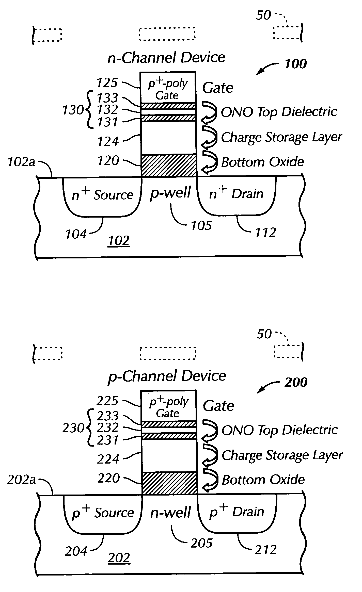
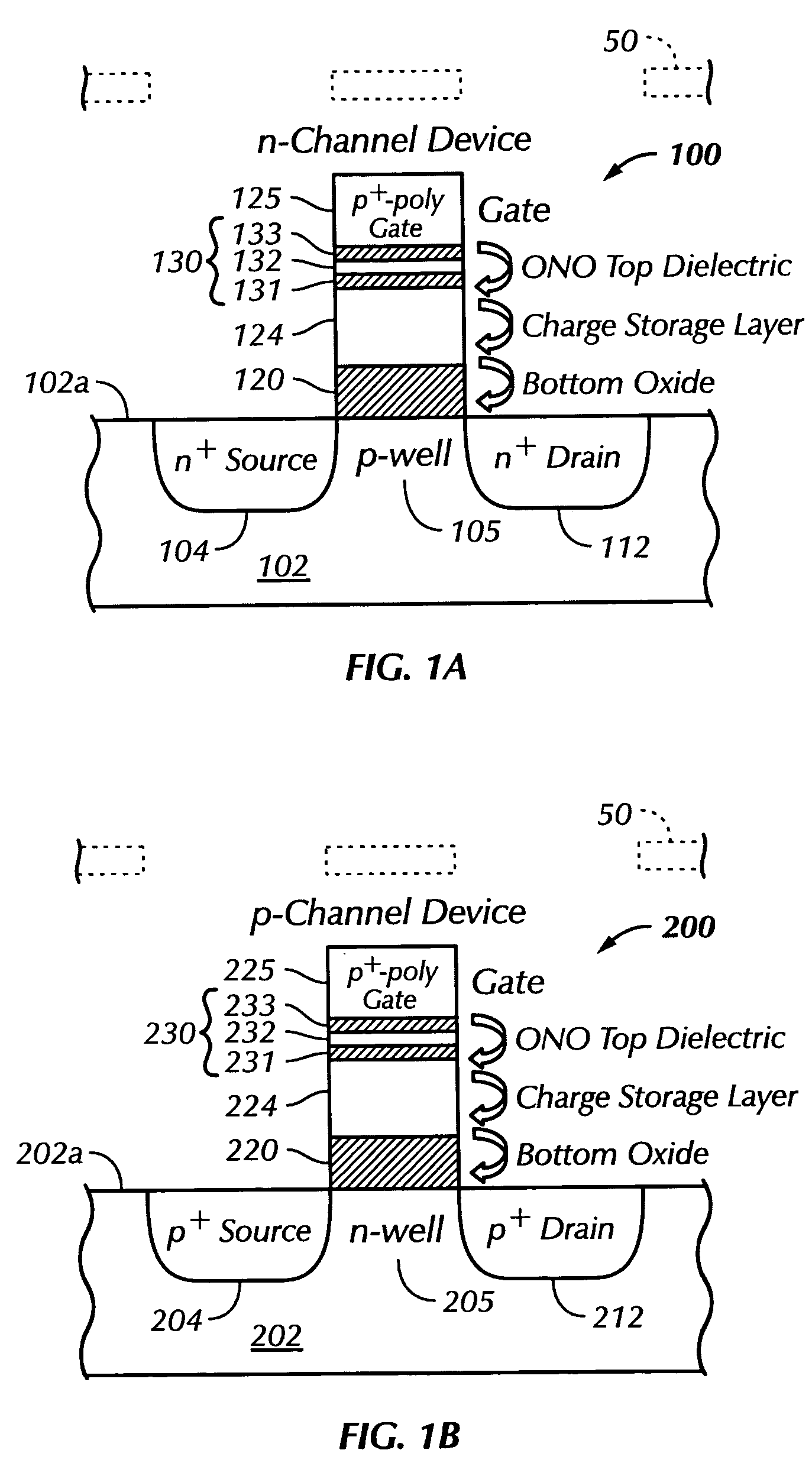
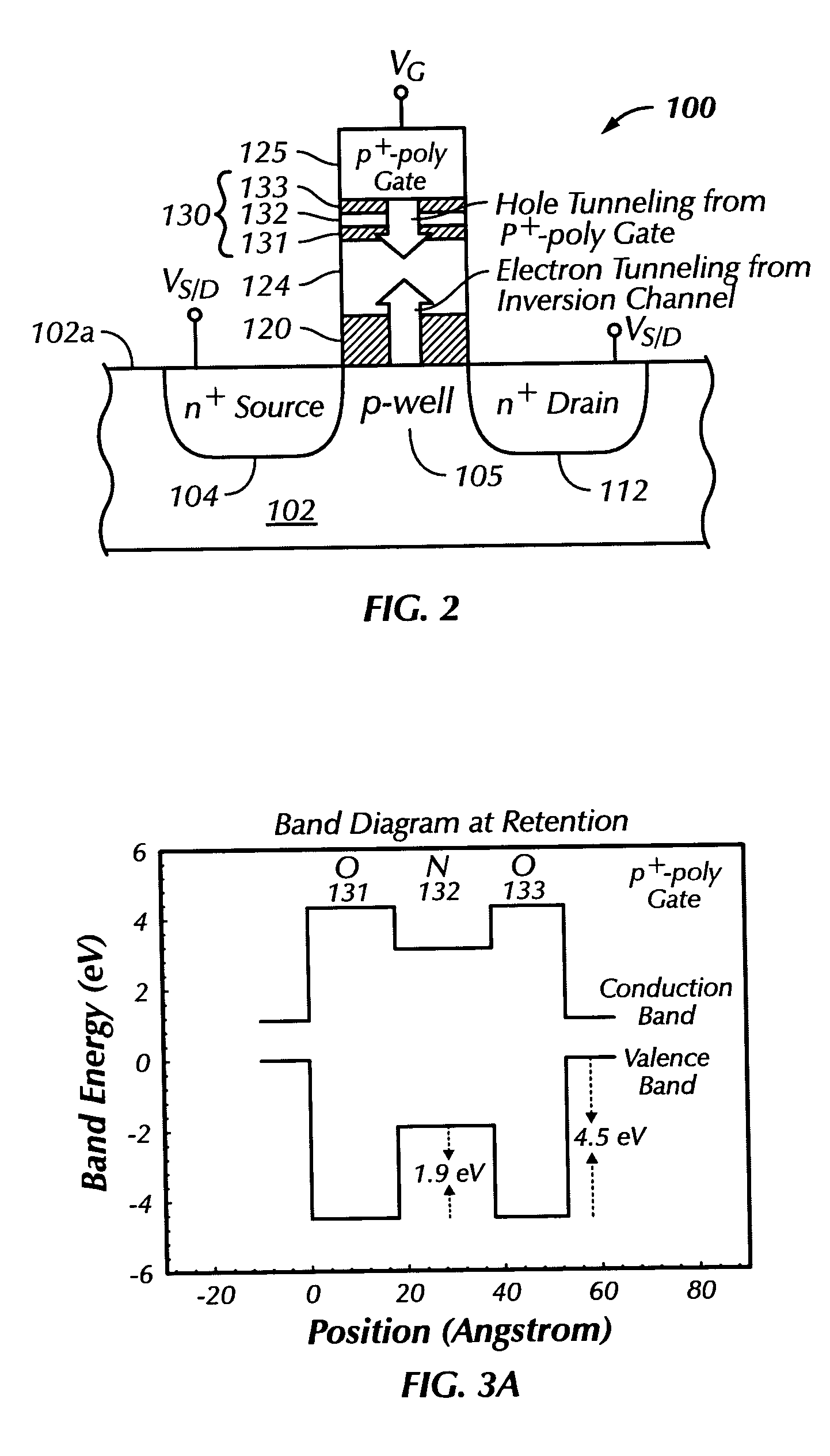
[0024] Certain terminology is used in the following description for convenience only and is not limiting. The words “right”, “left”, “lower”, and “upper” designate directions in the drawing to which reference is made. The words “inwardly” and “outwardly” refer direction toward and away from, respectively, the geometric center of the object described and designated parts thereof. The terminology includes the words above specifically mentioned, derivatives thereof and words of similar import. Additionally, the word “a,” as used in the claims and in the corresponding portions of the specification, means “at least one.”

[0025] One (1) micron or micrometer (μm) is 10,000 Angstroms (Å) or 1000 nanometers (mn).

[0026] As used herein, reference to conductivity will be limited to the embodiment described. However, those skilled in the art know that p-type conductivity can be switched with n-type conductivity and the device would still be functionally correct (i.e., a first or a second conduct...


PUM


Abstract

A non-volatile memory (NVM) cell includes a silicon substrate having a main surface, a source region in a portion of the silicon substrate, a drain region in a portion of the silicon substrate, and a well region disposed in a portion of the silicon substrate between the source and drain regions The cell includes a bottom oxide layer formed on the main surface of the substrate. The bottom oxide layer is disposed on a portion of the main surface proximate the well region. The cell includes a charge storage layer disposed above the bottom oxide layer, a dielectric tunneling layer disposed above the charge storage layer and a control gate formed above the dielectric tunneling layer. The dielectric tunneling layer includes a first oxide layer, a nitride layer and a second oxide layer. Erasing the NVM cell includes applying a positive gate voltage to inject holes from the gate.

Description

BACKGROUND OF THE INVENTION [0001] The present invention relates to a non-volatile memory semiconductor device and a method for manufacturing a non-volatile memory semiconductor device, and more particularly, to a non-volatile memory semiconductor device having an oxide-nitride-oxide (ONO) top dielectric layer and a method for manufacturing a non-volatile memory semiconductor device having an ONO top dielectric layer. [0002] Non-volatile memory (“NVM”) refers to semiconductor memory which is able to continually store information even when the supply of electricity is removed from the device containing such an NVM memory cell. NVM includes Mask Read-Only Memory (Mask ROM), Programmable Read-Only Memory (PROM), Erasable Programmable Read-Only Memory (EPROM) and Electrically Erasable Programmable Read-Only Memory (EEPROM). Typically, NVM can be programmed with data, read and / or erased, and the programmed data can be stored for a long period of time prior to being erased, even as long a...

Claims


Application Information

Patent Timeline
08 Feb 2007
Publication
US20070029625A1
IPC
H01L29/94; H01L29/76; H01L31/00; H10B69/00
CPC
H01L29/792; H01L29/513
Inventors
LUE, HANG-TING; LAI, ERH-KUN