Multilayer laminated circuit board

a multi-layer, circuit board technology, applied in the direction of inductance, printed electric component incorporation, electrical apparatus construction details, etc., can solve the problems of reducing the size of the multi-layer transformer package and the amount of wiring between the multi-layer transformer and other components, so as to improve the magnetic saturation characteristic, reduce the bending of the magnetic sheet on the peripheral edge and in the center of the dielectric sheet, and improve the effect of manufacturing

Inactive Publication Date: 2007-02-08
TAMURA KK
View PDF3 Cites 78 Cited by
  • Summary
  • Abstract
  • Description
  • Claims
  • Application Information

AI Technical Summary

Benefits of technology

[0035] According to the multi-layer transformer in the multi-layer laminated circuit board in a preferred embodiment of the present invention, the magnetic frame is aligned with the peripheral edge of the dielectric sheet, the magnetic core is aligned with the through hole in the center of the dielectric sheet, and the magnetic frame and magnetic core are sandwiched between the pair of magnetic sheets. As a result, bending of the magnetic sheets on the peripheral edge and in the center of the dielectric sheet can be reduced. Hence, there is little or no need to bend the magnetic sheets, and therefore manufacture can be made easier. Moreover, a magnetic path having a sufficient sectional area can be secured, enabling an improvement in the magnetic saturation characteristic.
[0036] According to the multi-layer transformer in the multi-layer laminated circuit board in a preferred embodiment of the present invention, the magnetic frame and magnetic core are connected via a support portion to form a magnetic sheet, and hence the magnetic frame and magnetic core can be formed simultaneously, and positioning thereof during lamination can also be performed simultaneously. Thus manufacture can be made easier.
[0037] According to the multi-layer transformer in the multi-layer laminated circuit board in a preferred embodiment of the present invention, the dielectric pattern of the composite sheet is formed between the primary winding and secondary winding, the magnetic patterns are formed in the center and on the peripheral edge of the composite sheet, and the pair of magnetic sheets contact each other through the magnetic patterns to form a core. As a result, a multi-layer transformer having a non-magnetic layer between the primary winding and secondary winding can be realized, and magnetic flux leakage can be suppressed. Moreover, in contrast to the conventional multi-layer transformer, there is no need to form a dielectric layer by coating the primary winding and secondary winding with a dielectric paste, and hence the insulating property between the primary windings and between the secondary windings does not deteriorate and the gap between the primary winding and secondary winding does not widen. As a result, the electromagnetic coupling coefficient can be increased while maintaining the insulating property between the windings. In addition, the insulating property between the primary winding and the secondary winding is enhanced by the interposition of the dielectric pattern in place of the conventional magnetic sheet.
[0038] Further, by forming the dielectric pattern and magnetic patterns on a single composite sheet, the number of sheets can be reduced and the lamination method can be simplified in comparison with a case in which a dielectric sheet constituted by a dielectric body alone and a magnetic sheet constituted by a magnetic body alone are laminated to form an identical structure.
[0039] In addition, according to the multi-layer transformer in the multi-layer laminated circuit board in a preferred embodiment of the present invention, by interposing an identical sheet to the aforementioned composite sheet between the primary winding or secondary winding and the magnetic sheet, the primary winding or secondary winding can be electrically protected, and hence the insulating property can be enhanced.
[0040] According to the multi-layer transformer in the multi-layer laminated circuit board in a preferred embodiment of the present invention, the film thickness of the magnetic patterns and the film thickness of the dielectric pattern are equal, and therefore the film thickness of the composite sheet is constant in all locations. As a result, the pair of magnetic sheets sandwiching the composite sheet can be made even, and hence a circuit pattern or the like can be formed on the magnetic sheets with a high degree of precision.

Problems solved by technology

However, limits have been reached in reducing the size of the multi-layer transformer package and reducing the amount of wiring between the multi-layer transformer and other components.

Method used


Image

  • Multilayer laminated circuit board
  • Multilayer laminated circuit board
  • Multilayer laminated circuit board

Examples


first embodiment

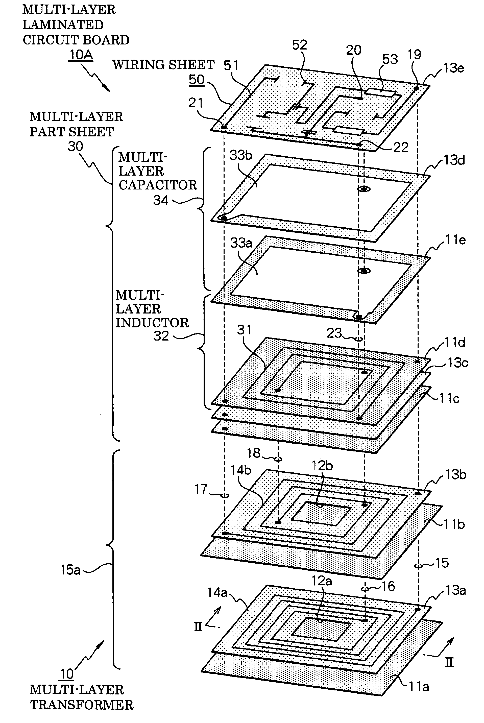
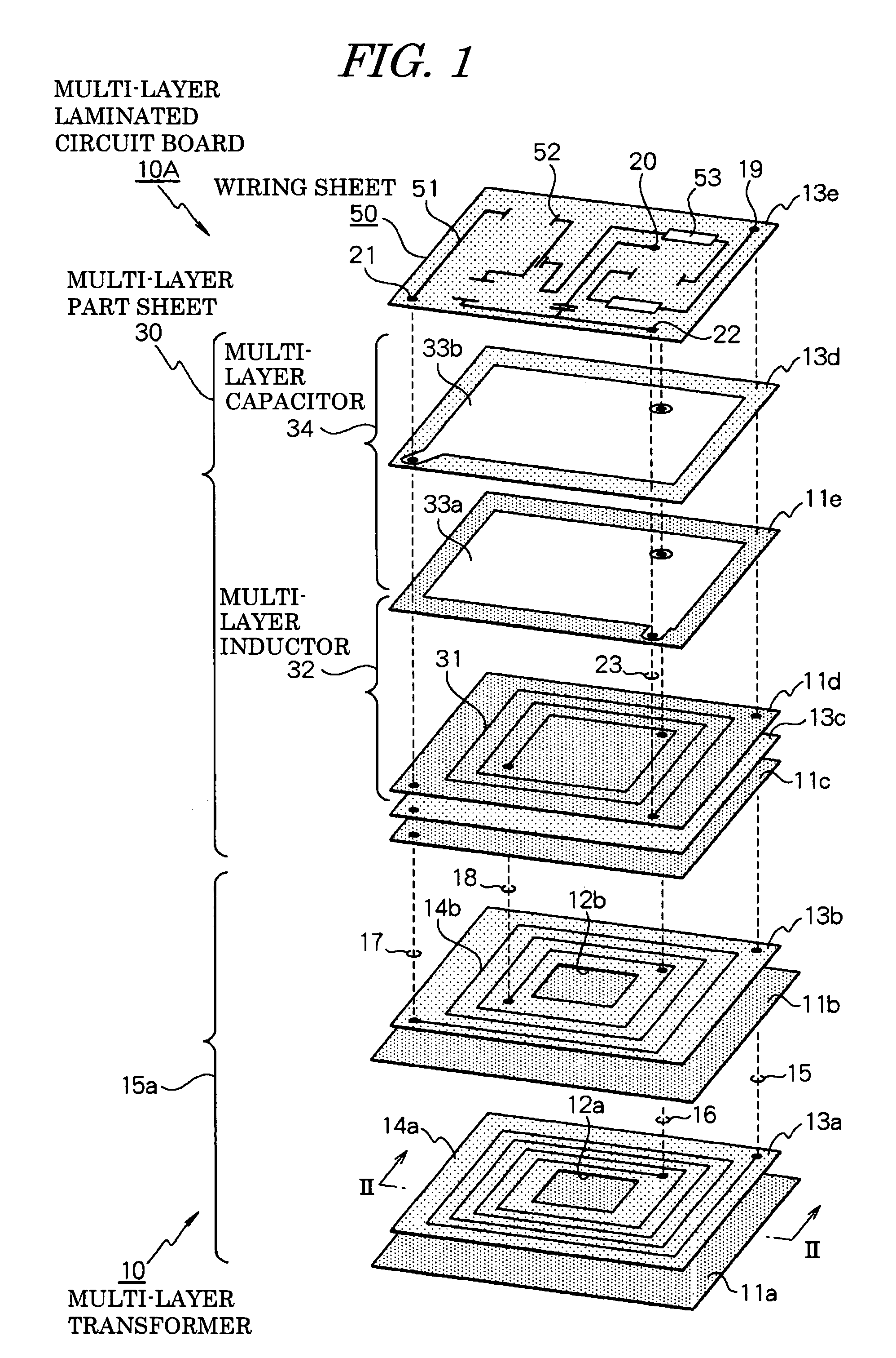
[0048]FIG. 1 is an exploded perspective view showing a multi-layer laminated circuit board according to the present invention. FIG. 2 is a longitudinal sectional view taken along a line II-II in FIG. 1 following lamination. The following description is based on these drawings.

third embodiment

[0049] A multi-layer laminated circuit board 10A according to this embodiment is formed by laminating in sequence a multi-layer transformer 10, a multi-layer part sheet 30 on which a multi-layer part is formed, and a wiring sheet 50 on which a circuit pattern is formed. In the multi-layer laminated circuit board 10A, the multi-layer transformer 10 is in-built, and therefore a package for the multi-layer transformer 10 is omitted and the wiring between the multi-layer transformer 10 and other components is reduced to a minimum. The reason for this is that the entire multi-layer laminated circuit board 10A is packaged, and therefore a package for the multi-layer transformer 10 is not required. Further, since wiring can be provided in the lamination direction, the surface area occupied by the wiring is reduced, and hence the wiring between the multi-layer transformer 10 and other components is reduced to a minimum. Moreover, the multi-layer transformer 10 may be provided on a part of t...

second embodiment

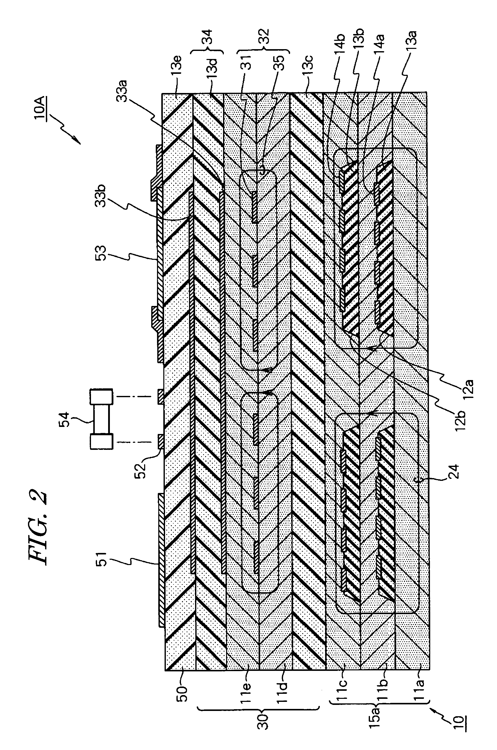
[0059]FIG. 3 is a partial sectional view showing the multi-layer laminated circuit board according to the present invention. The following description is based on this drawing. Note, however, that identical reference symbols have been allocated to parts that are identical to those of FIGS. 1 and 2, and description thereof has been omitted.

[0060] A multi-layer transformer 60 in the multi-layer laminated circuit board of this embodiment is constituted by further laminating laminated bodies 15b, . . . onto the laminated body 15a. The magnetic sheet 11c is shared by both of the laminated bodies 15a and 15b. Similarly to the laminated body 15a, the laminated body 15b comprises magnetic sheets 11c, 11f, 11g, dielectric sheets 13f, 13g, a primary winding 14c, and a secondary winding 14d. Further, although not shown in the drawing, through holes connecting the primary windings 14a, 14c. . . to each other and through holes connecting the secondary windings 14b, 14d, . . . to each other are p...


PUM

PropertyMeasurementUnit
thicknessaaaaaaaaaa
thicknessaaaaaaaaaa
thicknessaaaaaaaaaa

Abstract

A multi-layer laminated circuit board 10A of the present invention is formed by laminating together a multi-layer transformer 10, a multi-layer part sheet 30 formed with a multi-layer part, and a wiring sheet 50 formed with a circuit pattern. The multi-layer transformer 10 is incorporated into the multi-layer laminated circuit board 10A, and therefore a package for the multi-layer transformer 10 is omitted, and the wiring between the multi-layer transformer 10 and other components is reduced to a minimum.

Description

TECHNICAL FIELD [0001] The present invention relates to a multi-layer laminated circuit board in the field of semiconductor technology, more specifically, relates to that having an in-built multi-layer transformer in which a coil and core are formed by stacking sheets having electromagnetic characteristics. BACKGROUND ART [0002] In recent years, multi-layer transformers have attracted attention that are thin, small, and lightweight in accordance with rapid advances in the miniaturization of electronic devices. FIG. 13 is a disassembled perspective view of a stacked body of a conventional multi-layer transformer. FIG. 14 is a vertical cross-sectional view along the line XIV-XIV in FIG. 13 after stacking. The description below is based on FIGS. 13 and 14. [0003] A conventional multi-layer transformer 80 comprises primary-winding magnetic sheets 82b and 82d on which primary windings 81a and 81c are formed, secondary-winding magnetic sheets 82c and 82e on which secondary windings 81b an...

Claims


Application Information

Patent Timeline
Patent Type & Authority Applications(United States)
IPC IPC(8): H05K1/16H01F17/00H01F27/28H05K3/46
CPCH01F17/0013H01F27/2804H05K3/4688H05K1/165H05K3/4611H01F2017/0066
Inventor SUZUKI, YUKIHARUKOBAYASHI, TOSHIHIKOMIZOGUCHI, TOSHIMI
Owner TAMURA KK
Why Eureka
Try Eureka