Semiconductor memory module with error correction

a memory module and memory module technology, applied in the direction of printed circuit aspects, instruments, electric digital data processing, etc., can solve the problems of not being able to implement and not being desirable, and achieve the effect of simple and space-saving manner

Inactive Publication Date: 2007-02-08
POLARIS INNOVATIONS LTD
View PDF20 Cites 29 Cited by
  • Summary
  • Abstract
  • Description
  • Claims
  • Application Information

AI Technical Summary

Benefits of technology

[0021] Briefly, a semiconductor memory module having on-board error correction is provided in which the ECC memory chips are connected to a control chip via a control bus in a simple and space-saving manner. In one embodiment, the semiconductor memory module comprises a module circuit board having at least one an internal layer having a first surface and a second surface. A plurality of memory chips are provided each comprising a memory cell array having memory cells for storing data. First and second groups of the plurality of memory chips are arranged on the first surface of the module circuit board. A designated one of the plurality of memory chips stores data for error correction purposes. This is a so-called ECC memory chip. A control chip on the first surface of the circuit board drives the plurality of memory chips with control signals and corrects data read out erroneously from memory cells of the memory chips in the first group or second group of memory chips based on data for error correction that is stored in the designated memory chip. The designated memory chip is arranged on the first surface of the module circuit board between the control chip and the first and second groups of memory chips.

Problems solved by technology

Therefore, it is not possible to implement the branches of the partial buses CAB1 and CAB2 (for connecting the ECC memory chips to the control chip) in accordance with the standard shown in FIG. 3.
In a 2R×4 module configuration this situation arises particularly when the input and output terminals of the control chip HC do not conform to a standard.
This is not desirable.

Method used


Image

  • Semiconductor memory module with error correction
  • Semiconductor memory module with error correction
  • Semiconductor memory module with error correction

Examples


Embodiment Construction

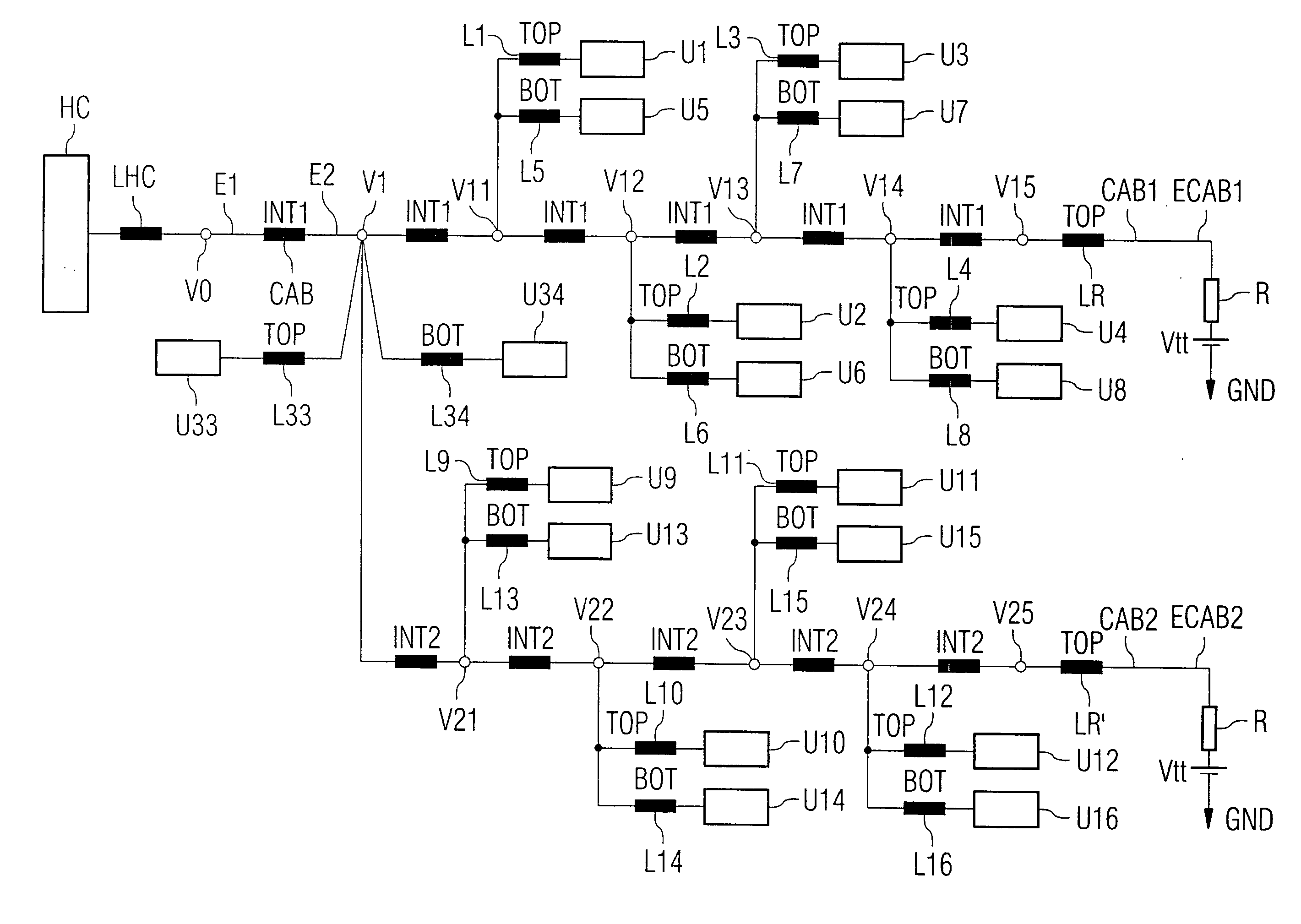
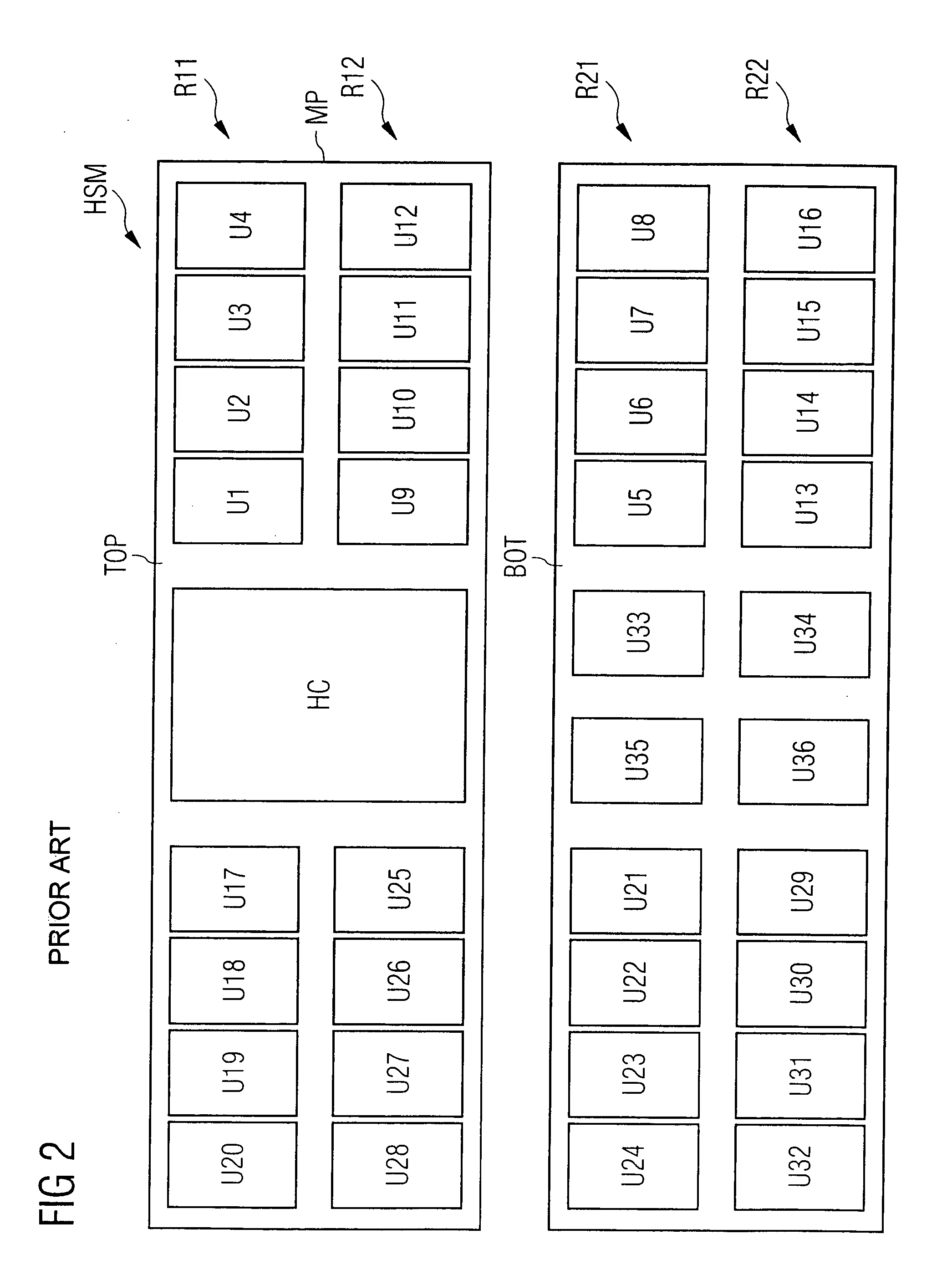
[0031] Reference is first made to FIG. 6 that shows a semiconductor memory module HSM of the 2R×4 module configuration and chip positioning scheme according to an embodiment of the present invention. FIG. 6 shows a positioning arrangement for a control chip HC, memory chips that are designated ECC memory chips U33, U34, U35 and U36 and a plurality of memory chips U1, . . . , U32 in accordance with one aspect of the invention. The control chip HC is arranged in the center on the top side TOP (first surface) of the module circuit board MP. Either or both of the ECC memory chips (U33, U35) on the first surface of the circuit board MP is also referred to herein as a first designated memory chip and either or both of the ECC memory chips (U34, U36) on the second surface of the circuit board MP is also referred to herein as a second designated memory chip. The semiconductor memory module HSM may be a fully buffered dual in-line memory module.

[0032] The plurality of memory chips are group...


PUM


Abstract

A semiconductor memory module comprises a control chip for driving ECC memory chips and further memory chips. The memory chips are arranged in two rows on a top side and a bottom side of the module circuit board. The ECC memory chips are arranged centrally on the module circuit board alongside the rows of the memory chips. A control bus connects the ECC memory chips and also the memory chips to the control chip. In a region remote from the control chip, the control bus branches in a contact-making hole into a first partial bus, to which a first group of memory chips are connected, and a second partial bus, to which a second group of memory chips are connected. The ECC memory chips are likewise connected to the control bus via the contact-making hole. Since the ECC memory chips are not arranged directly under the control chip, a bus branch directed backward is not required. As a result, space considerations on the module circuit board are eased and signal integrity on the control buses is improved.

Description

CROSS REFERENCE TO RELATED APPLICATIONS [0001] This application claims priority under 35 USC §119 to German Application No. DE 102005033710.4, filed Jul. 19, 2005, and entitled “Semiconductor Memory Module with Error Correction,” the entirety of which is incorporated herein by reference. FIELD OF THE INVENTION [0002] The present invention relates to a semiconductor memory module with an error correction, in which an ECC (error correcting code) memory chip is connected to a control chip via a control bus. BACKGROUND OF THE INVENTION [0003]FIG. 1 shows a conventional memory chip U, which is embodied for example as a DRAM (dynamic random access memory) memory chip. The memory chip U comprises a memory cell array SZF, in which memory cells SZ are arranged in matrix-like fashion along word lines WL and bit lines BL. A memory cell SZ comprises a selection transistor AT and a storage capacitor SC. In the case of a read or write access, the selection transistor AT is controlled to be put in...

Claims


Application Information

Patent Timeline
Patent Type & Authority Applications(United States)
IPC IPC(8): G11C29/00
CPCG06F11/1044G11C5/025H05K1/181H05K2201/10159H05K2201/09254H05K2201/09627H05K3/429Y02P70/50
Inventor MOOSRAINER, KARL-HEINZDJORDJEVIC, SRDJANBESTELE, MICHAEL
Owner POLARIS INNOVATIONS LTD
Why Eureka
Try Eureka