Printed wiring board fabrication method, printed wiring board photomask, and program for creating a photomask
a technology of printed wiring and fabrication methods, applied in the direction of printed circuits, electrical devices, cable/conductor manufacturing, etc., can solve the problems of inability to control the wiring pattern to a predetermined width, production efficiency, and the amount of etching to become comparatively larg
- Summary
- Abstract
- Description
- Claims
- Application Information
AI Technical Summary
Benefits of technology
Problems solved by technology
Method used
Image

Examples
embodiment 1
[0066] First, the fabrication method for a printed wiring board according to an embodiment of the present invention will be described.
[0067] A substrate of a printed wiring board is constituted from insulating resin such as, for example, glass epoxy resin or paper phenol resin. On the surface of the substrate, metal foil, for example copper foil, is formed. Next, a dry film photoresist is applied on the metal foil, a photomask is overlaid, and by irradiating ultraviolet rays, an etching resist is formed. Next, a portion that is not covered by the etching resist is etched by an etching solution. Afterward, a wiring pattern is formed by removing the etching resist, completing the printed wiring board.
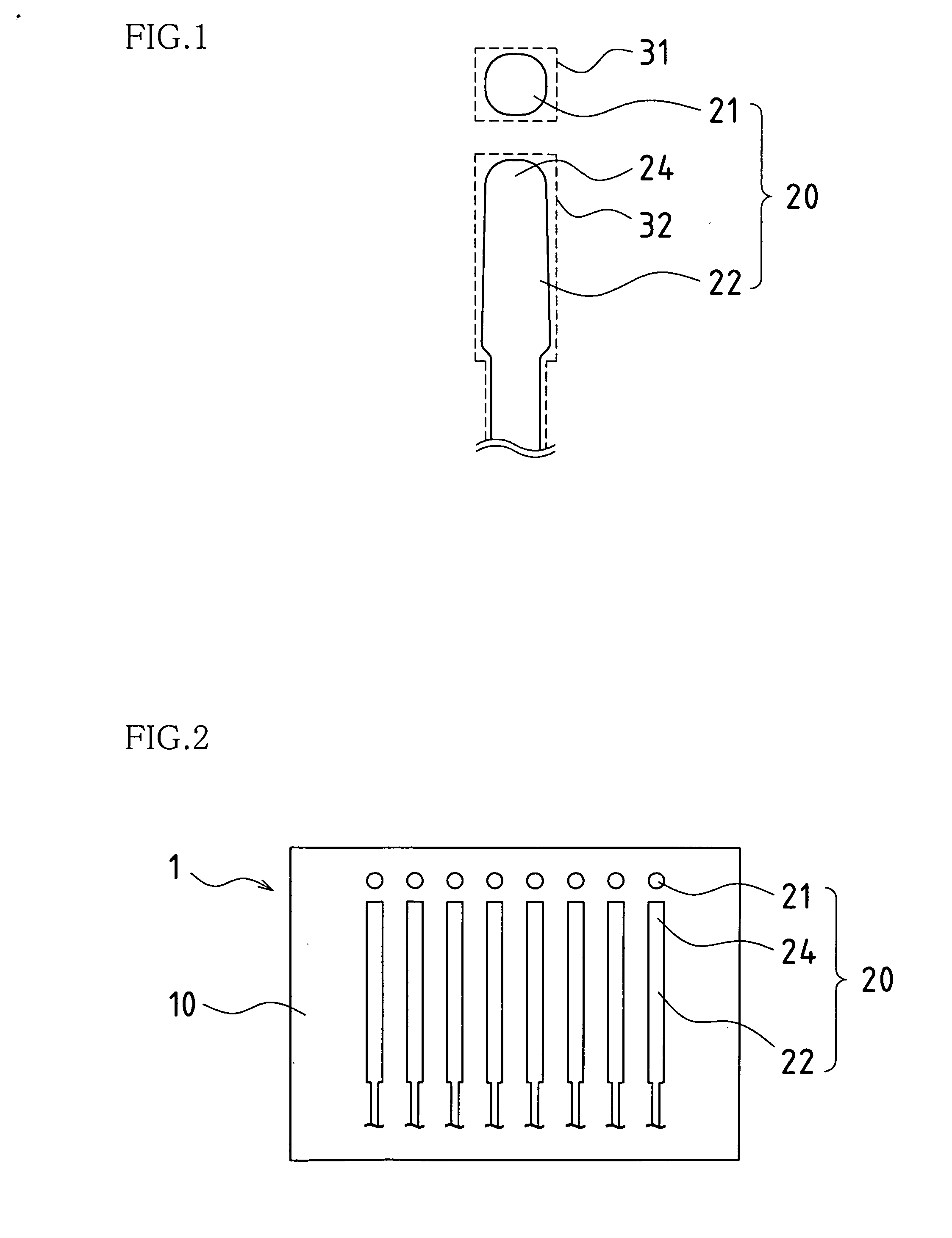
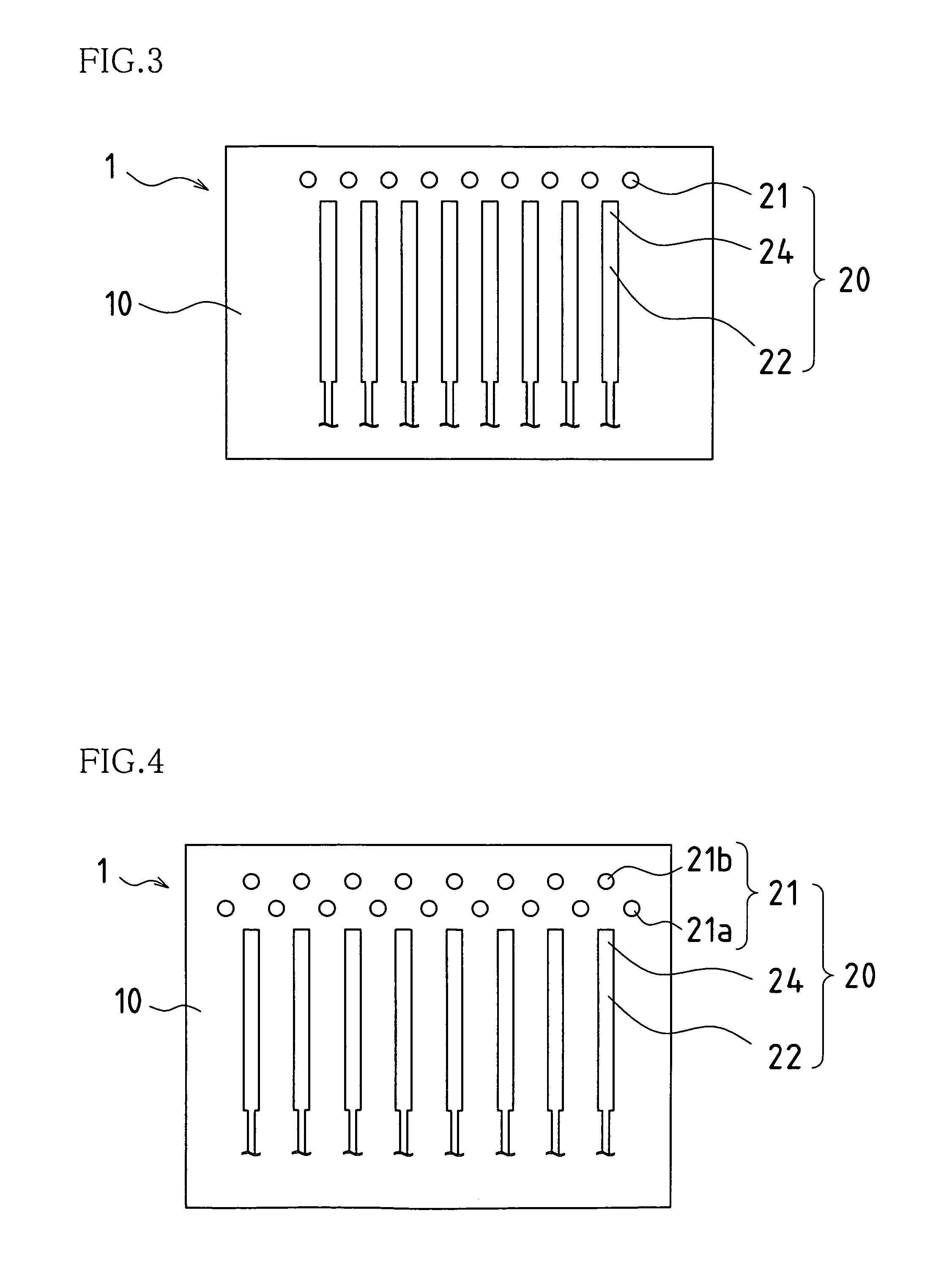
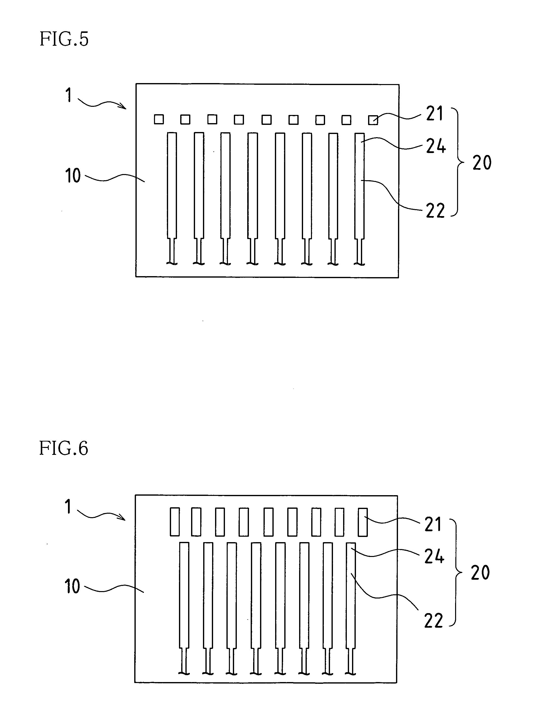
[0068] The wiring pattern is configured from a circuit pattern that constitutes an electric circuit and a dummy pattern that is not necessary in order to constitute an electric circuit. The circuit pattern, for example, is configured from a land connected to a terminal of a semiconducto...
embodiment 2
[0089] Next is a description of a photomask for the printed wiring board according to the present invention, with reference to FIGS. 1 to 7.
[0090] In the photomask, a mask pattern for forming the wiring pattern 20 is formed. As described in Embodiment 1, the wiring pattern 20 is configured from a circuit pattern that constitutes an electric circuit, and the dummy pattern 21, which is not necessary in order to constitute the electric circuit. On the other hand, the mask pattern is configured from a circuit mask pattern and a dummy mask pattern that correspond to the circuit pattern and the dummy pattern 21.
[0091] When fabricating the printed wiring board 1, by using this sort of photomask, a photoresist that corresponds to the circuit pattern and the dummy pattern 21 is formed, and it is possible to create the printed wiring board 1 having the circuit pattern and the dummy pattern 21.
embodiment 3
[0092] Next is a description of the photomask creation program according to the present invention, with reference to FIGS. 1 to 7.
[0093] The photomask creation program is configured from a circuit module that forms a circuit mask pattern from a circuit pattern that constitutes an electric circuit, a dummy module that forms a dummy mask pattern that corresponds to the dummy pattern 21, and a combining portion that combines the circuit mask pattern and the dummy mask pattern.
[0094] The circuit module creates a circuit mask pattern for a circuit pattern that is input to the photomask creation program.
[0095] The dummy module designs positions at which it is possible to dispose dummy patterns 21, the shape of the dummy pattern 21, and the like based on the circuit pattern that is input to the photomask creation program, and creates a corresponding dummy mask pattern based on the designed dummy mask pattern 21.
[0096] Also, the circuit mask pattern and the dummy mask pattern are combin...
PUM
 Abstract
Description
Claims
Application Information
 - R&D
- Intellectual Property
- Life Sciences
- Materials
- Tech Scout
- Unparalleled Data Quality
- Higher Quality Content
- 60% Fewer Hallucinations
Browse by: Latest US Patents, China's latest patents, Technical Efficacy Thesaurus, Application Domain, Technology Topic, Popular Technical Reports.
© 2025 PatSnap. All rights reserved.Legal|Privacy policy|Modern Slavery Act Transparency Statement|Sitemap|About US| Contact US: help@patsnap.com