In-situ atomic layer deposition

a dielectric layer and atomic layer technology, applied in the direction of coatings, chemical vapor deposition coatings, metallic material coating processes, etc., can solve the problems of deposited dielectric layers that are undensified and can cause contamination, and achieve good electrical properties and good uniformity

Inactive Publication Date: 2007-02-15
TOKYO ELECTRON LTD
View PDF10 Cites 424 Cited by
  • Summary
  • Abstract
  • Description
  • Claims
  • Application Information

AI Technical Summary

Benefits of technology

[0008] The invention provides an in situ method for forming a HfO2 high-k dielectric layer with good uniformity and good electrical properties in a batch wafer processing system, where the wafers are not transferred between process chambers between pre-deposition oxidation treatments, atomic layer deposition, and post-deposition annealing. The method of the invention comprises first loading a plurality of wafers into a process chamber, and then pre-treating the plurality of wafers in the process chamber with a first oxidizer selected from an oxygen-containing gas or an oxygen- and nitrogen-containing gas. After pre-treating the wafers, and without removing the wafers from the process chamber, the method then comprises depositing HfO2 on the plurality of wafers by atomic layer deposition. The atomic layer deposition comprises a plurality of deposition cycles, each cycle comprising alternating exposure of the plurality of wafers in the process chamber to a second oxidizer and a hafnium precursor with optional purging in-between. The second oxidizer is selected from an oxygen-containing gas or an oxygen- and nitrogen-containing gas, and the hafnium precursor is selected from hafnium tert-butoxide (HTB) or hafnium tetra-diethylamide (TDEAH). After deposition, the wafers are unloaded from the process chamber.

Problems solved by technology

With each transfer of the wafers, contamination can occur.
In addition, without the post-treatment, the deposited dielectric layer is undensified, and may be harmed by exposure to air during the wafer transfer from the deposition system to the post-treatment system.

Method used


Image

  • In-situ atomic layer deposition
  • In-situ atomic layer deposition
  • In-situ atomic layer deposition

Examples


Embodiment Construction

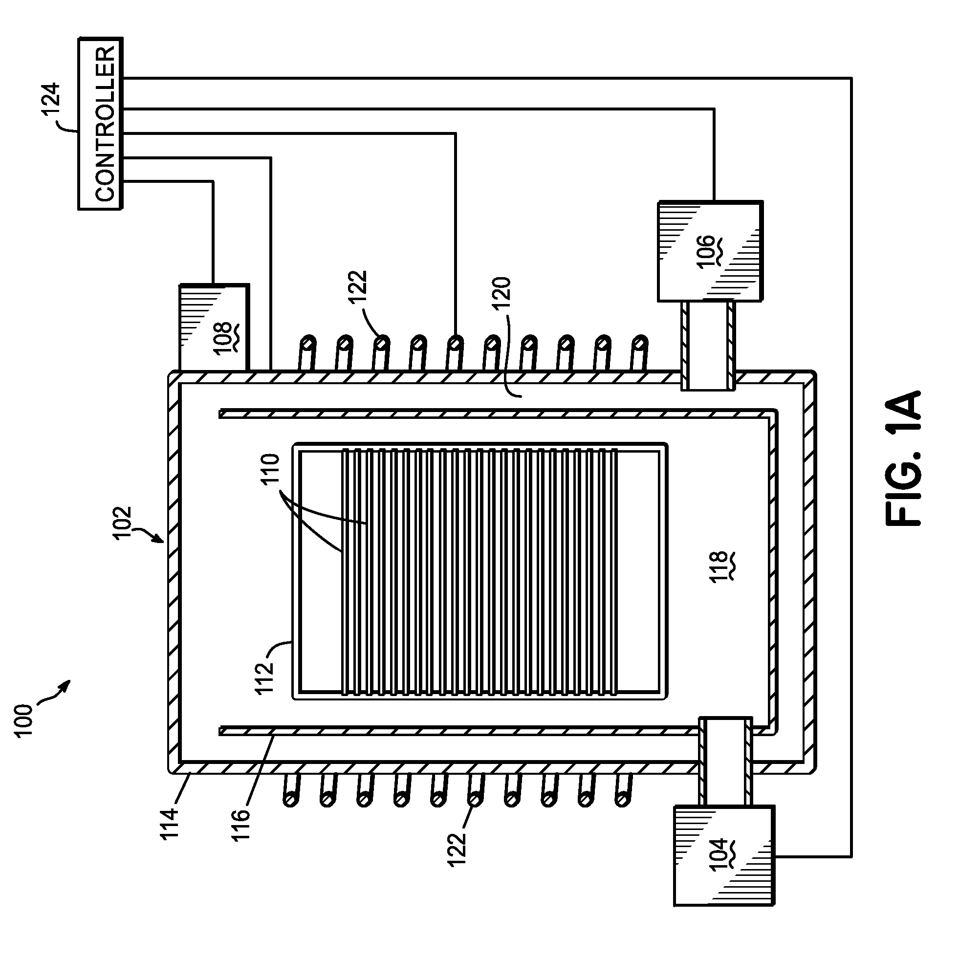
[0027] The present invention is directed to in-situ atomic layer deposition of an HfO2 high-k dielectric layer in a batch wafer processing system. The process includes a pre-oxidation treatment, followed by deposition by alternate exposures to an oxidizer and a hafnium tert-butoxide (HTB) or hafnium tetra-diethylamide (TDEAH) precursor, the structures of which are depicted in FIG. 4. The chamber may be purged between oxidizing and precursor exposure, and between repeating cycles of exposure to the oxidizer and precursor, and the cycles may be repeated a desired number of times. The purging process may use an inert gas, for example, such as H2 or Ar. The purge time may be any desired time for removing excess reactant from the chamber, for example, about 10 seconds to about 5 minutes, and by way of further example, about 30 seconds to about 2 minutes.

[0028] The oxidizer for the pre-oxidization treatment and for the deposition may be the same or different, and may be an oxygen-contain...


PUM

PropertyMeasurementUnit
temperatureaaaaaaaaaa

Abstract

An in situ method for forming a HfO2 high-k dielectric layer in a batch wafer processing system. The method comprises first loading a plurality of wafers into a process chamber, and then pre-treating the plurality of wafers in the process chamber with a first oxidizer. After pre-treating the wafers, and without removing the wafers from the process chamber, the method then comprises depositing HfO2 on the plurality of wafers by atomic layer deposition, which comprises a plurality of deposition cycles, each cycle comprising alternating exposure of the plurality of wafers in the process chamber to a second oxidizer and a hafnium precursor. The hafnium precursor is selected from hafnium tert-butoxide (HTB) or hafnium tetra-diethylamide (TDEAH).

Description

FIELD OF THE INVENTION [0001] This invention relates to atomic layer deposition of an HfO2 high-k dielectric layer, and more particularly to an in-situ process including pre-oxidation, atomic layer deposition of the HfO2 dielectric layer, and a post-deposition anneal. BACKGROUND OF THE INVENTION [0002] Several methods have been developed for creating thin films on substrates used in manufacturing semiconductor devices. Among the more established techniques is Chemical Vapor Deposition (CVD). Atomic Layer Deposition (ALD), a variant of CVD, is a relatively newer technology now emerging as a potentially superior method of achieving uniform, conformal film deposition. [0003] ALD has demonstrated an outstanding ability to maintain ultra-uniform thin deposition layers over complex topology. This is at least partially true because ALD is not as flux dependent as is CVD. This flux-independent nature of ALD allows processing at lower temperatures than with conventional CVD methods. [0004] T...

Claims


Application Information

Patent Timeline
Patent Type & Authority Applications(United States)
IPC IPC(8): H01L21/31
CPCC23C16/0236C23C16/405C23C16/45546H01L21/31645C23C16/56H01L21/3141C23C16/45553H01L21/02323H01L21/02205H01L21/02312H01L21/0228H01L21/02181H01L21/02318H01L21/02337
Inventor DIP, ANTHONYSASAKI, SADAOTOELLER, MICHAELREID, KIMBERLY G.
Owner TOKYO ELECTRON LTD
Why Eureka
Try Eureka