Electron beam irradiating apparatus

Inactive Publication Date: 2007-02-22
NGK INSULATORS LTD
View PDF8 Cites 33 Cited by
  • Summary
  • Abstract
  • Description
  • Claims
  • Application Information

AI Technical Summary

Benefits of technology

[0040] According to the present invention, it is possible to provide an electron beam irradiating apparatus

Problems solved by technology

However, the above conventional electron beam irradiating apparatus has the following problems to be solved.
Firstly, there is a problem in that an electron beam (thermion) is irradiated from one filament in many cases and thus, a irradiation range is narrow.
Accordingly, a large amount of electrons pass through the object to be irradiated to cause a problem of low efficiency.
Further, there are problems in that the apparatus structure has to be complicated for scanning and in that the power supply device needs to be upsized for applying the beam with the high energy, and it is also necessary to shield an X-ray resulting therefrom.
However, in practice, the numbers of filaments and grids that may be provided inside the terminal are limited.
This leads to another problem that the physical property of the object to be irradiated which would be changed as a result of irradiation with

Method used


Image

  • Electron beam irradiating apparatus
  • Electron beam irradiating apparatus
  • Electron beam irradiating apparatus

Examples


first embodiment

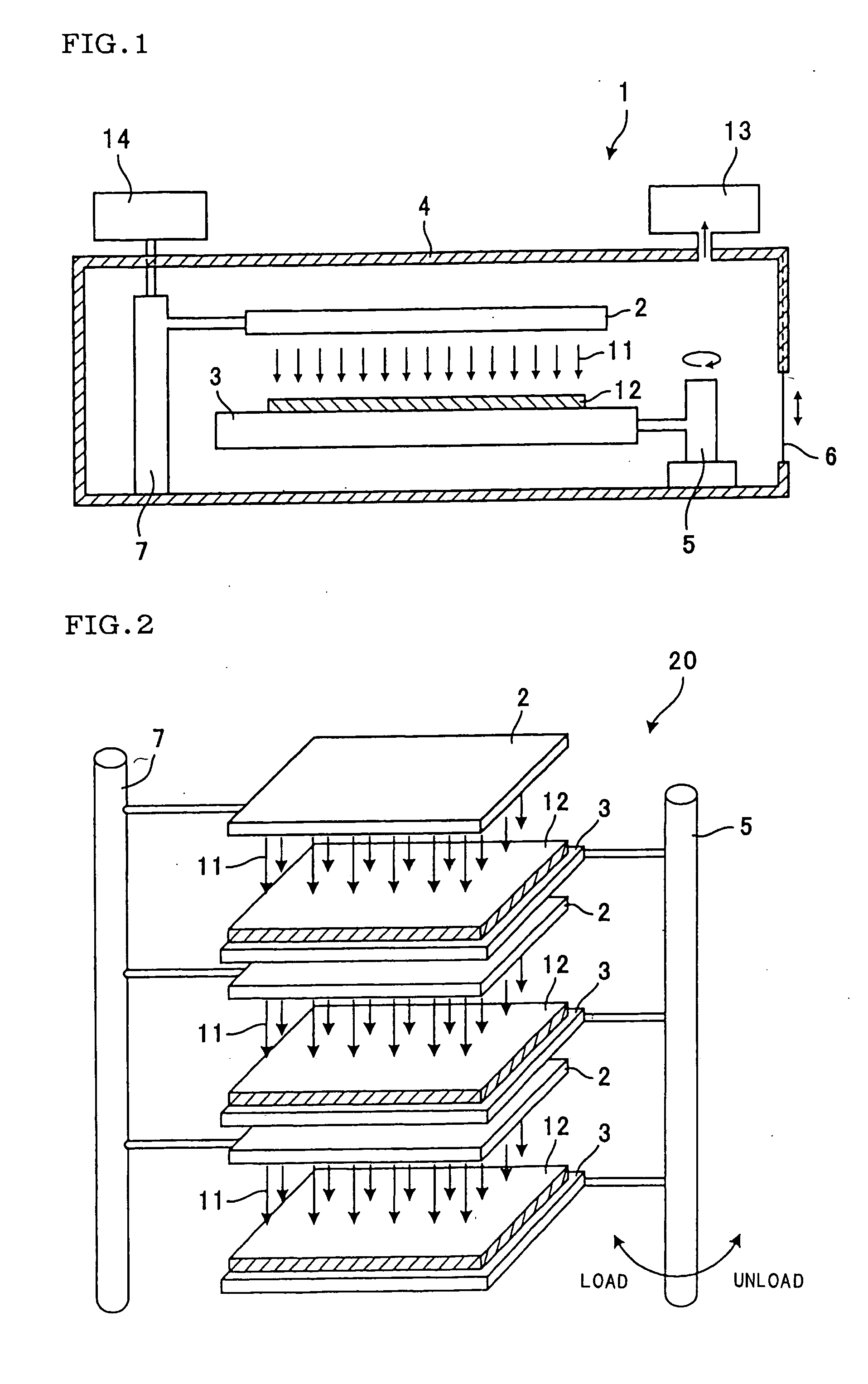
[0055]FIG. 1 is a sectional view of an electron beam irradiating apparatus according to the present invention. FIGS. 7 and 8 are partial enlarged views of a planar electron emitting element as a component of the electron beam irradiating apparatus according to the present invention. FIG. 7 is a photograph showing a surface of the planar electron emitting element on the first electrode side. FIG. 8 is a partial sectional view of the planar electron emitting element. In FIG. 7, black portions represent through-holes.

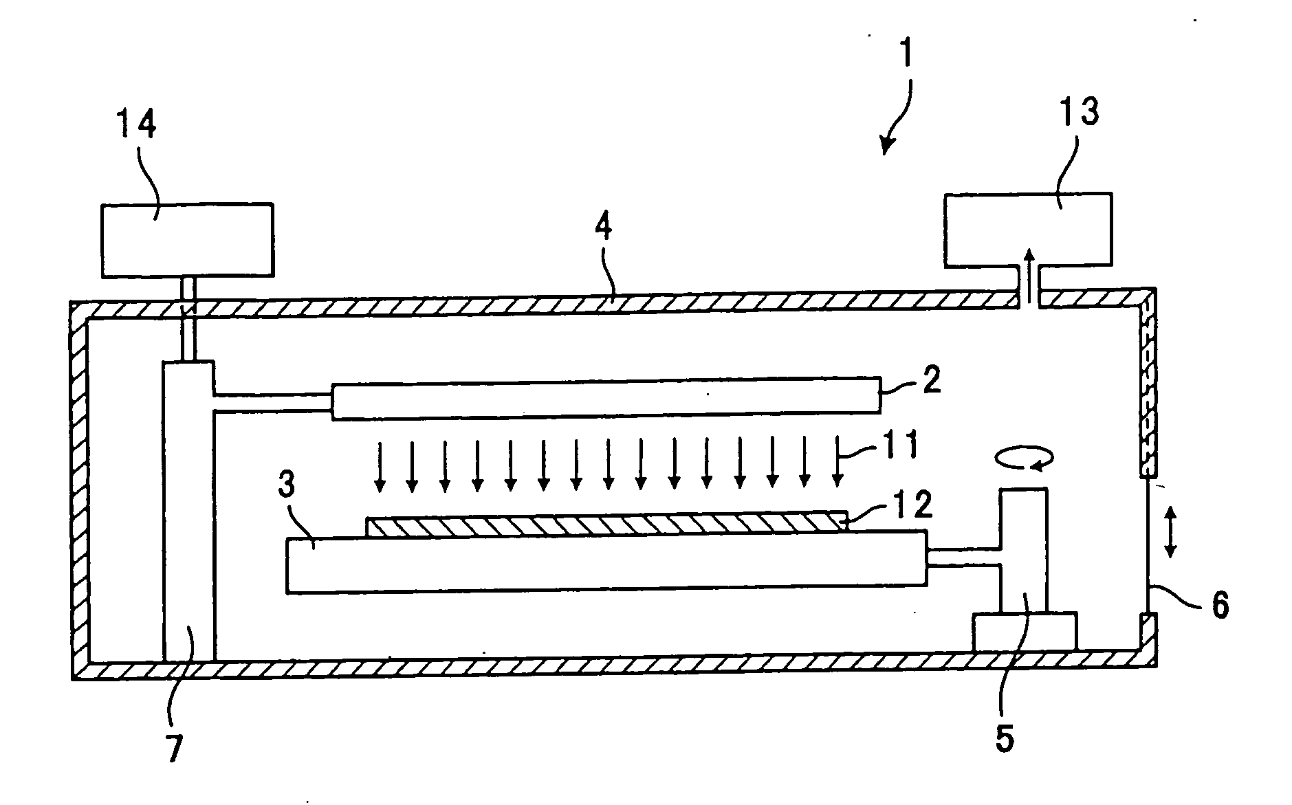
[0056] An electron beam irradiating apparatus 1 shown in FIG. 1 includes a planar electron emitting element for generating and emitting an electron beam 11, an object to be irradiated 12 (for example, wafer on which a porous silicon oxide film is formed) which is irradiated with the electron beam 11, and a stage 3 (positioning means) where the object to be irradiated is mounted. The element, the object to be irradiated, and the stage are provided in a chamber 4 that is kep...

third embodiment

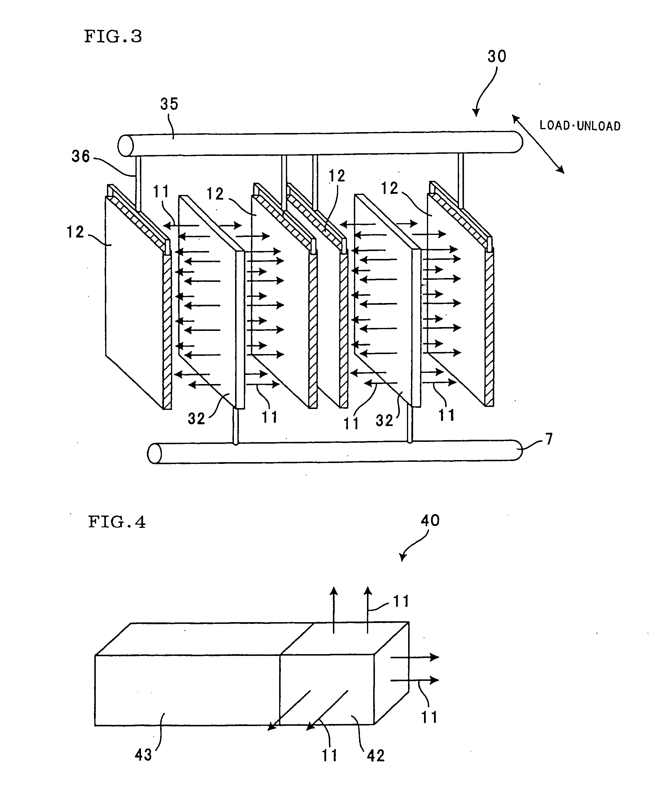
[0072] An electron beam irradiating apparatus 30 according to the present invention as shown in FIG. 3 includes two planar electron emitting elements 32 for generating and emitting the electron beam 11, and conveying mechanisms 35 (positioning means) having four suspenders 36 that suspend the four objects to be irradiated 12. In the electron beam irradiating apparatus 30, the electron beam 11 emitted from both surfaces of the two planar electron emitting elements 32 is applied to the four objects to be irradiated 12. Although the chamber and shutter are not shown in FIG. 3, the suspended objects to be irradiated 12 may be loaded / unloaded together with the suspenders 36 to / from the chamber 4 along with the linear rotation of the conveying mechanism 35.

[0073] In the electron beam irradiating apparatus 30, an emitter portion 91 of the electron emitting elements 32 has a sheet-like shape having two surfaces from which electrons (e−) are emitted. The planar electron emitting elements 32 ...

fourth embodiment

[0074]FIG. 4 only shows a planar electron emitting element 42 and a supporting member 43 for supporting the element in an electron beam irradiating apparatus 40 according to the invention. The planar electron emitting element 42 of FIG. 4 has a polyhedral surface for emitting the electron beams 11. The polyhedral surface forms rectangle. The electron beam 11 may be emitted to five directions (except the supporting member 43 side). In the planar electron emitting element 42, a first electrode is formed on an outer surface of the inner emitter portion. A second electrode is formed inside the emitter portion. In the electron beam irradiating apparatus 40 thus configured, for example, a robot hand is placed in a chamber for holding the supporting member 43 to control the direction of the planar electron emitting element 42, whereby the electron beam may be applied in every directions to the object to be irradiated that is loaded in the chamber. Accordingly, a desired change in physical ...


PUM


Abstract

An electron beam irradiating apparatus includes a chamber being kept under vacuum, and housing a planar electron emitting element and a positioning unit and an object to be irradiated is directly irradiated with an electron beam emitted from the element. The planar electron emitting element includes: an emitter portion composed of a dielectric material; and a first electrode and a second electrode applied with a driving voltage for emitting electrons, and the first electrode is formed on a first surface of the emitter portion and has a plurality of through-holes where the emitter portion is exposed, a surface of the first electrode facing to the emitter portion around the through-holes is separated from the emitter portion, and the electron beam is emitted from the first surface of the emitter portion through the through-holes.

Description

BACKGROUND OF THE INVENTION [0001] 1. Field of the Invention [0002] The present invention relates to an electron beam irradiating apparatus for generating an electron beam and applying the generated electron beam to an object to be irradiated to change physical properties of the object to be irradiated. [0003] 2. Description of the Related Art [0004] In recent years, there have been placed great expectations on an electron beam irradiating apparatus. The electron beam irradiating apparatus may be used as means for sterilizing drinking water or decomposing and removing harmful substances as well as means that contributes to our safety and health. This apparatus has recently come to play an important role especially in a semiconductor manufacturing process. This is because existing techniques face limit in increasing an integration degree of devices and improving an operational speed of the devices while following a conventional manufacturing method using a photolithography step (resi...

Claims


Application Information

Patent Timeline
IPC IPC(8): A61N5/00
CPCG21K5/04H01L21/67005H01J37/317
Inventor NANATAKI, TSUTOMUOHWADA, IWAOBESSHO, YUKIAKAO, TAKAYOSHI
Owner NGK INSULATORS LTD
Why Eureka
Try Eureka