Polishing pad and method of manufacture

a polishing pad and manufacturing method technology, applied in the direction of manufacturing tools, grinding devices, other chemical processes, etc., can solve the problems of polishing pads that are not made according to the method, polishing pads that lose surface asperities with use, and pores that wear away and become clogged with debris

Active Publication Date: 2007-02-22
ROHM & HAAS ELECTRONICS MATERIALS CMP HLDG INC
View PDF14 Cites 23 Cited by
  • Summary
  • Abstract
  • Description
  • Claims
  • Application Information

AI Technical Summary

Benefits of technology

[0013] A first aspect of the invention provides a method of manufacturing a polishing pad useful for polishing substrates in a chemical mechanical polishing process using a polishing composition, the method comprising the steps of: preparing a polymeric matrix material; mixing polymeric capsules into the polymeric matrix material to distribute the polymeric capsules within the polymeric matrix material, the polymeric capsules comprising a polymeric shell and a liquid core contained within the polymeric shell; and forming a polishing pad, the polishing pad having the polymeric capsules distributed in the formed polymeric matrix material, the polymeric shell holding the liquid core to prevent contact with the polymeric matrix material during forming, and the polymeric shell having a polishing surface that ruptures to create surface asperities for polishing the substrates.

Problems solved by technology

As the conditioned polishing pad is used, the pores wear away and become clogged with debris from the CMP process.
This results in the polishing pad losing surface asperities with use.
Polishing pads made according to the '362 patent, however, suffer from the tendency of the capsules to expand.
The amount of expansion is difficult to control for two reasons.
The other factor that makes capsule expansion hard to control is the effect of differential heating.
Uneven expansion of the capsules results in non-uniform pad porosity, and therefore non-uniform pad density, which is disadvantageous.

Method used


Image

  • Polishing pad and method of manufacture
  • Polishing pad and method of manufacture
  • Polishing pad and method of manufacture

Examples


Embodiment Construction

[0018] The present invention provides a method of manufacturing a polishing pad useful for planarizing a substrate in a chemical mechanical polishing process with increased ease and efficiency.

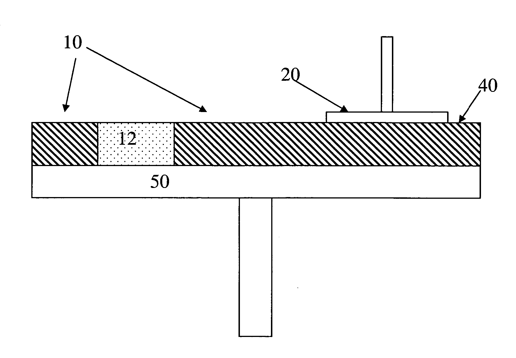
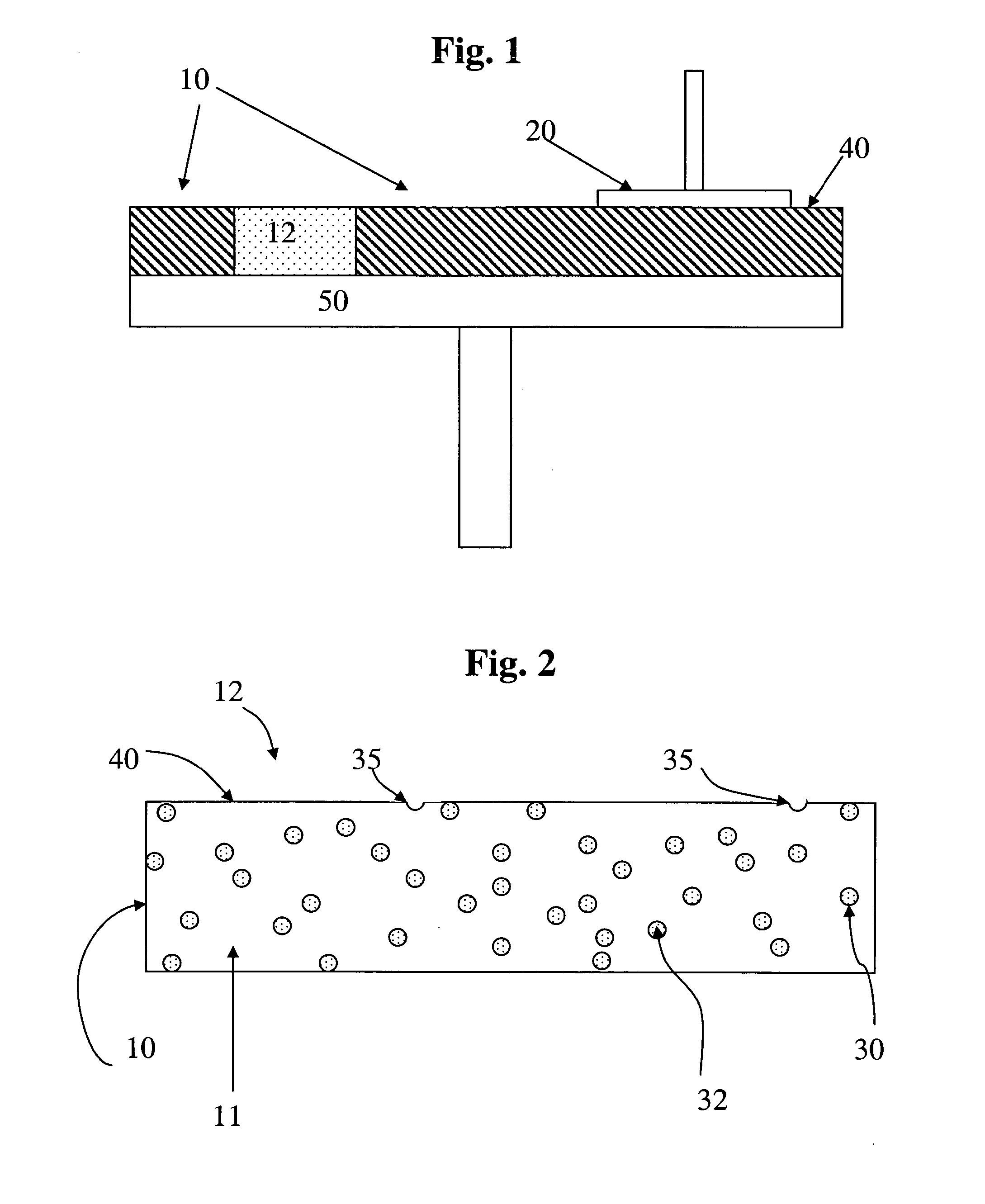
[0019] Referring to FIG. 1, a polishing pad 10 of the present invention is shown mounted on a platen 50. The polishing pad 10 has a polishing surface 40 that is contacted with a substrate 20, such as a patterned silicon wafer. Also shown is a region of the polishing pad 12 that is shown in greater detail in FIG. 2

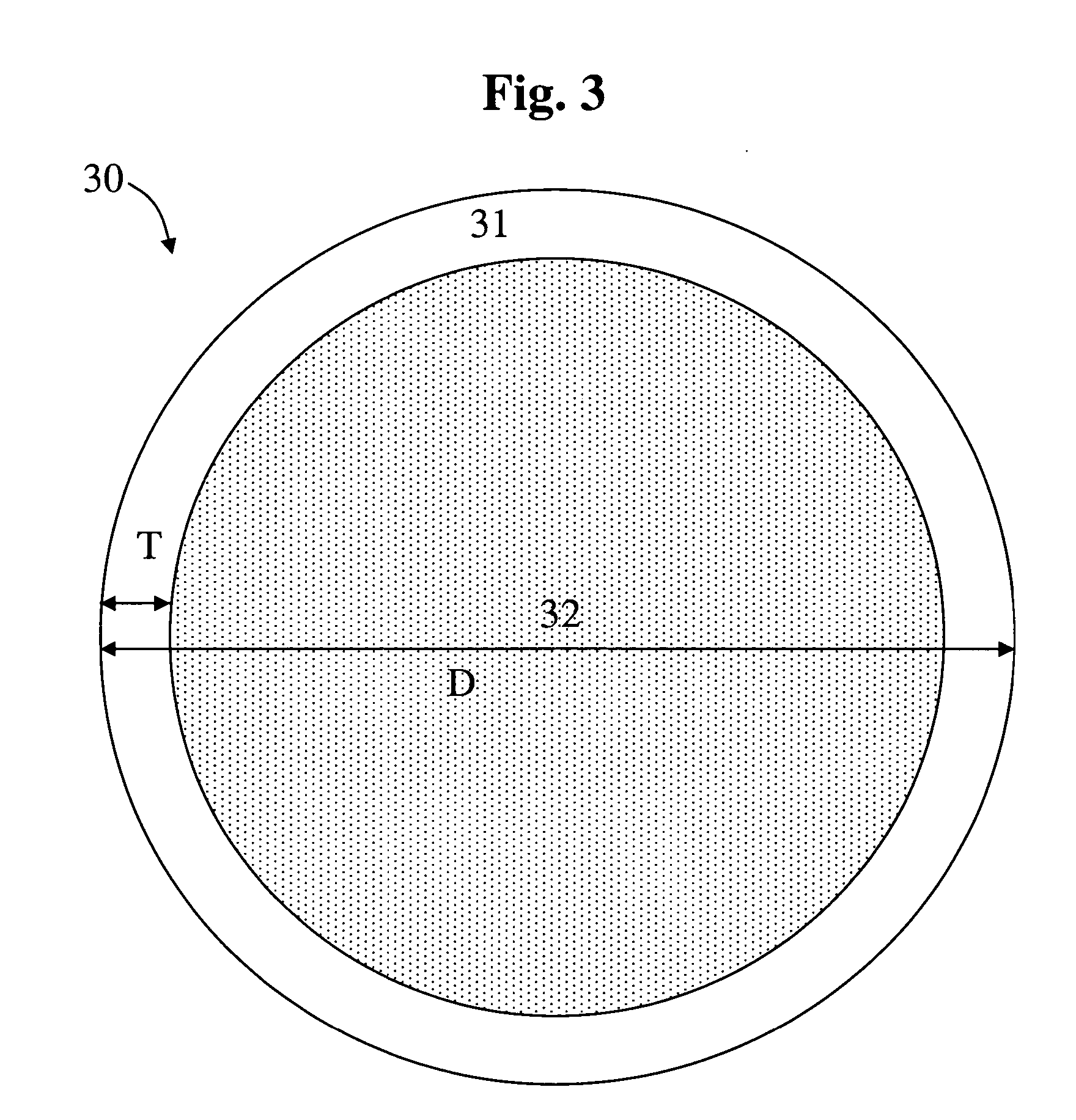
[0020] Referring now to FIG. 2, the method comprises preparing a polymeric matrix material 11, mixing polymeric capsules 30 into the polymeric matrix material 11 and forming a polishing pad 10. In particular, the polymeric capsules 30 have a polymeric shell 31 (FIG. 3) and a liquid core 32. The polymeric capsules 30 have increased density and increased resistance to expansion when exposed to heat during the manufacturing process. The result is a reduction in the tendency for the poly...


PUM

PropertyMeasurementUnit
thicknessaaaaaaaaaa
thicknessaaaaaaaaaa
thicknessaaaaaaaaaa

Abstract

The present invention relates to a method of manufacturing a polishing pad with embedded polymeric capsules useful for planarizing a substrate in a CMP process using a polishing composition. The method reduces non-uniformity of the polishing pad due to capsule floating, differential heating and capsule expansion by the use of novel capsule materials. The method also increases the efficiency of the manufacturing process by reducing the number of defective products and reducing waste.

Description

CROSS REFERENCE TO RELATED APPLICATION [0001] This application claims the benefit of U.S. Provisional Application Ser. No. 60 / 709,280 filed Aug. 18, 2005.BACKGROUND [0002] The present invention generally relates to a method of manufacturing a polishing pad useful for polishing and planarizing substrates using a chemical-mechanical planarization (“CMP”) process. More particularly, the method of the present invention improves uniformity both within the pad and from one pad to another. [0003] In the fabrication of integrated circuits and other electronic devices, multiple layers of conducting, semiconducting and dielectric materials are deposited on or removed from a surface of a semiconductor wafer. Thin layers of conducting, semiconducting, and dielectric materials may be deposited by a number of deposition techniques. Common deposition techniques in modern processing include physical vapor deposition, also known as sputtering, chemical vapor deposition, plasma-enhanced chemical vapo...

Claims


Application Information

Patent Timeline
Patent Type & Authority Applications(United States)
IPC IPC(8): B24D11/00B24B37/20B24D99/00C08J3/20H01L21/304
CPCB24B37/205B24D18/0009
Inventor SAIKIN, ALAN H.
Owner ROHM & HAAS ELECTRONICS MATERIALS CMP HLDG INC
Why Eureka
Try Eureka