Method of manufacturing wiring board

a manufacturing method and technology of wiring boards, applied in the field of manufacturing wiring boards, can solve the problems of difficult to achieve a thinner design and higher density of wiring boards, and achieve the effects of reducing manufacturing time, facilitating manufacturing process, and reducing the thickness of the chip-built wiring boards

Active Publication Date: 2007-03-01
SHINKO ELECTRIC IND CO LTD
View PDF9 Cites 73 Cited by
  • Summary
  • Abstract
  • Description
  • Claims
  • Application Information

AI Technical Summary

Benefits of technology

[0009] An object of an embodiment of the invention is to achieve a thinner chip-built-in wiring board as well as to suppress warpage of the wiring board.
[0014] According to the method of the invention, the supporting board is removed after the insulating layer where a semiconductor chip is embedded and the wiring connected to the semiconductor chip are formed, and the first and second reinforcing layers are simultaneously formed so as to sandwich the insulating layer and the like where the supporting board is absent. In general, a reinforcing layer shows large shrinkage on curing. However, since the first and second reinforcing layers are simultaneously formed so as to sandwich the insulating layer, the shrinkage on curing is uniformly applied from above and below the insulating layer, thus preventing an occurrence of warpage.
[0016] According to the method of the invention, a prepreg material is used as a reinforcing layer. This makes it easy to form the reinforcing layer as well as enhance the rigidity of the reinforcing layer.
[0020] According to the method of the invention, removal of a supporting board is stopped by the stop layer thus preventing removal of the supporting board from having an effect on the layers that are inside of the stop layer. Control of removal processing in removing the supporting board is made easy, and thus the manufacture of a wiring board is simplified.
[0026] According to the method of the invention, it is possible to simultaneously form layers that are formed on and under the insulating layer, thus the manufacturing process is facilitated and time required for manufacture is reduced.
[0027] According to the method of the invention, it is possible to provide a thinner chip-built-in wiring board that suppress a warpage in the wiring board.

Problems solved by technology

A possible warpage of a wiring board has presented a problem in a case where a chip built-in wiring board with a thinner design and higher packing density is to be provided.
In such a laminated structure, it is difficult to achieve a thinner design and higher density of a wiring board.

Method used


Image

  • Method of manufacturing wiring board
  • Method of manufacturing wiring board
  • Method of manufacturing wiring board

Examples


Embodiment Construction

[0049] A preferred embodiment of the invention will be described referring to drawings.

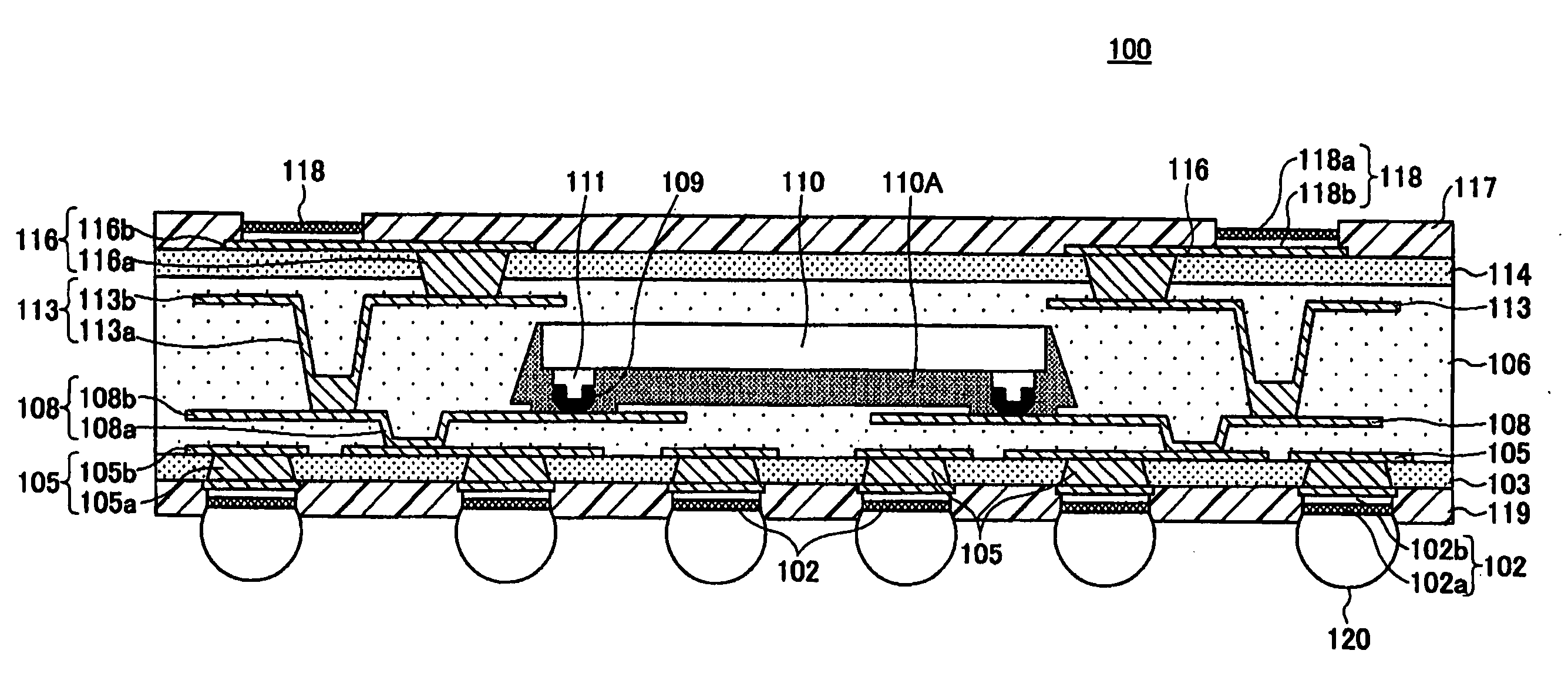
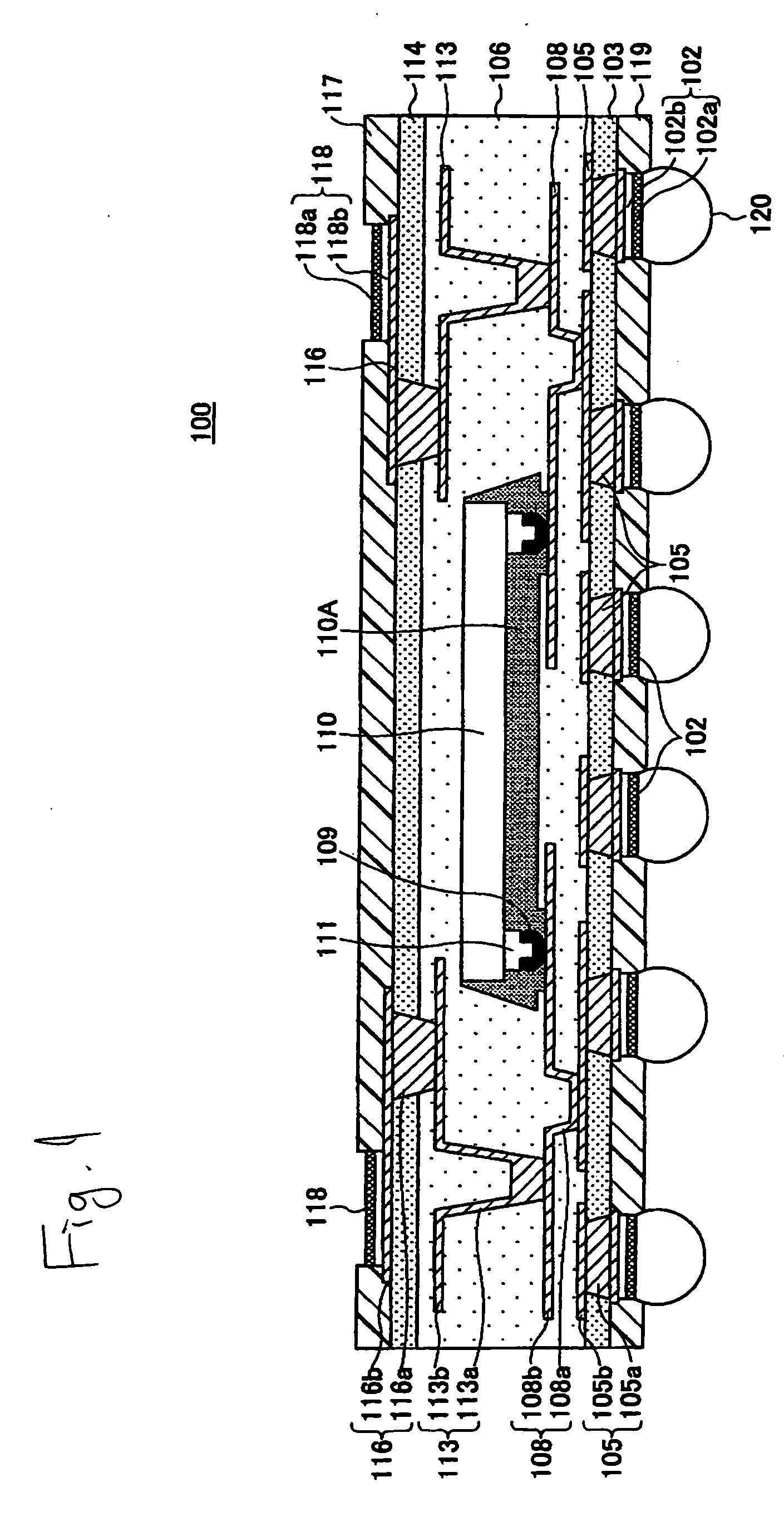
[0050]FIG. 1 is a schematic cross-sectional view of a wiring board 100 manufactured by a method of manufacturing a wiring board as an embodiment of the invention. For the purpose of explanation, the structure of the wiring board 100 will be described before describing the method of manufacturing the wiring board 100.

[0051] As shown in FIG. 1, the wiring board 100 manufactured in this embodiment has an insulating layer 106 including a so-called buildup resin material such as epoxy where a semiconductor chip 110 is embedded. First and second reinforcing layers 103, 114 are formed with respect to the insulating layer 106.

[0052] The reinforcing layers 103, 104 are arranged so as to sandwich the insulating layer 106 from top and bottom as shown in the figure. The reinforcing layers 103, 114 are formed using a material having a high rigidity such as a prepreg material. The insulating layer 106 is for...


PUM

PropertyMeasurementUnit
elastic modulusaaaaaaaaaa
thickaaaaaaaaaa

Abstract

A method of manufacturing a wiring board including an insulating layer where a semiconductor chip is embedded includes: forming, on a supporting board, the insulating layer where the semiconductor chip is embedded and a wiring connected to the semiconductor chip; removing the supporting board by etching; and simultaneously forming first and second reinforcing layers so as to sandwich the insulating layer after removing the supporting board.

Description

[0001] This application claims foreign priority based on Japanese Patent application No. 2005-246438, filed Aug. 26, 2005, the content of which is incorporated herein by reference in its entirety. BACKGROUND OF THE INVENTION [0002] 1. Field of the Invention [0003] The present invention relates to a method of manufacturing a wiring board, and in particular to a wiring board in which a semiconductor chip is incorporated. [0004] 2. Description of the Related Art [0005] Nowadays, the performance of electronic apparatuses that use semiconductor devices such as semiconductor chips are being advanced, and as a result, there are demands for mounting semiconductor chips on a board at a higher density, and miniaturizing and downsizing the board to which the semiconductor chips are mounted. [0006] Thus, there have been proposed substrates in which semiconductor chips are built, so-called chip built-in wiring boards (for example, refer to JP-A-2004-327624) and various structures designed to bui...

Claims


Application Information

Patent Timeline
Patent Type & Authority Applications(United States)
IPC IPC(8): H05K1/11
CPCH01L21/4857H01L21/563H01L21/6835H01L23/5389H01L24/81H01L2221/68345H01L2224/1134H01L2224/13144H01L2224/16225H01L2224/73203H01L2224/73204H01L2224/81001H01L2224/81801H01L2224/82H01L2224/83001H01L2224/85H01L2224/86H01L2924/01078H01L2924/01079H01L2924/15311H01L2924/15331H01L2924/3511H05K1/186H05K3/20H05K3/4644H05K3/4688H05K2201/10674H01L2924/00014H01L2924/00013H01L2224/13099H01L2224/32225H01L2924/00H01L2924/15192Y10T29/4913Y10T29/49117Y10T29/49156Y10T29/49126Y10T29/53174Y10T29/49135Y10T29/49155Y10T29/49128Y10T29/49149H01L2924/12042H05K3/24
Inventor YAMANO, TAKAHARU
Owner SHINKO ELECTRIC IND CO LTD
Why Eureka
Try Eureka