Design of silicon-controlled rectifier by considering electrostatic discharge robustness in human-body model and charged-device model devices

a technology of electrostatic discharge and rectifier, which is applied in the direction of semiconductor/solid-state device details, diodes, transistors, etc., can solve the problems of ic protection, high cost of products, and damage or destruction of ics, and achieve enhanced esd protection capabilities and low voltage triggered

Inactive Publication Date: 2007-03-01
ORTIZ & LOPEZ PLLC +1
View PDF18 Cites 15 Cited by
  • Summary
  • Abstract
  • Description
  • Claims
  • Application Information

AI Technical Summary

Benefits of technology

[0011] The following summary of the invention is provided to facilitate an understanding of some of the innovative features unique to the present invention and is not intended to be a full description. A full appreciation of the various aspects of the invention can be gained by taking the entire specification, claims, drawings and abstract as a whole.
[0012] It is therefore one aspect of the present invention to provide for an improved silicon-controlled rectifier utilized for ESD protection.
[0013] It is another aspect of the present invention to provide for an improved low voltage triggered silicon-controlled rectifier.
[0014] It is a further aspect of the present invention to provide for a low voltage triggered silicon-controlled rectifier with enhanced ESD protection capabilities with performance enhancements thereof under human-body model (HBM) and charged-device model (CDM) stress conditions.
[0015] It is y

Problems solved by technology

A semiconductor integrated circuit (IC) is generally susceptible to an electrostatic discharge (ESD) event that may damage or destroy the IC.
In deep sub-micron, or small geometry, complementary metal oxide silicon (CMOS) technology, the protection of an IC becomes an even more important issue due to the implementation of thin oxide layers in such ICs.
During installation of integrated circuits into products, these electrostatic discharges may destroy the IC's and thus require expensive repairs on the products, which could have been avoided by providing a mechanism for dissipation of the electrostatic discharge to which the IC may have been subjected.
The ESD problem has been especially pronounced in complementary metal oxide semiconductor (CMOS) field effect transistors.
One of the problems inherent with low voltage triggered SCR's, such as, for example, LVTSCR 100 and LVTSCR 200, is that due to a slow turn-on time in the lateral SCR, the lateral n-p-n BJT of ggNMOSFET's can become damaged as a result of associated positive and negative CDM events.
Thus, although low voltage triggered SCR's are very robust in human-body model (HBM) stress conditions, such devices are very weak in CDM stress conditions.

Method used


Image

  • Design of silicon-controlled rectifier by considering electrostatic discharge robustness in human-body model and charged-device model devices
  • Design of silicon-controlled rectifier by considering electrostatic discharge robustness in human-body model and charged-device model devices
  • Design of silicon-controlled rectifier by considering electrostatic discharge robustness in human-body model and charged-device model devices

Examples


Embodiment Construction

[0025] The particular values and configurations discussed in these non-limiting examples can be varied and are cited merely to illustrate embodiments of the present invention and are not intended to limit the scope thereof.

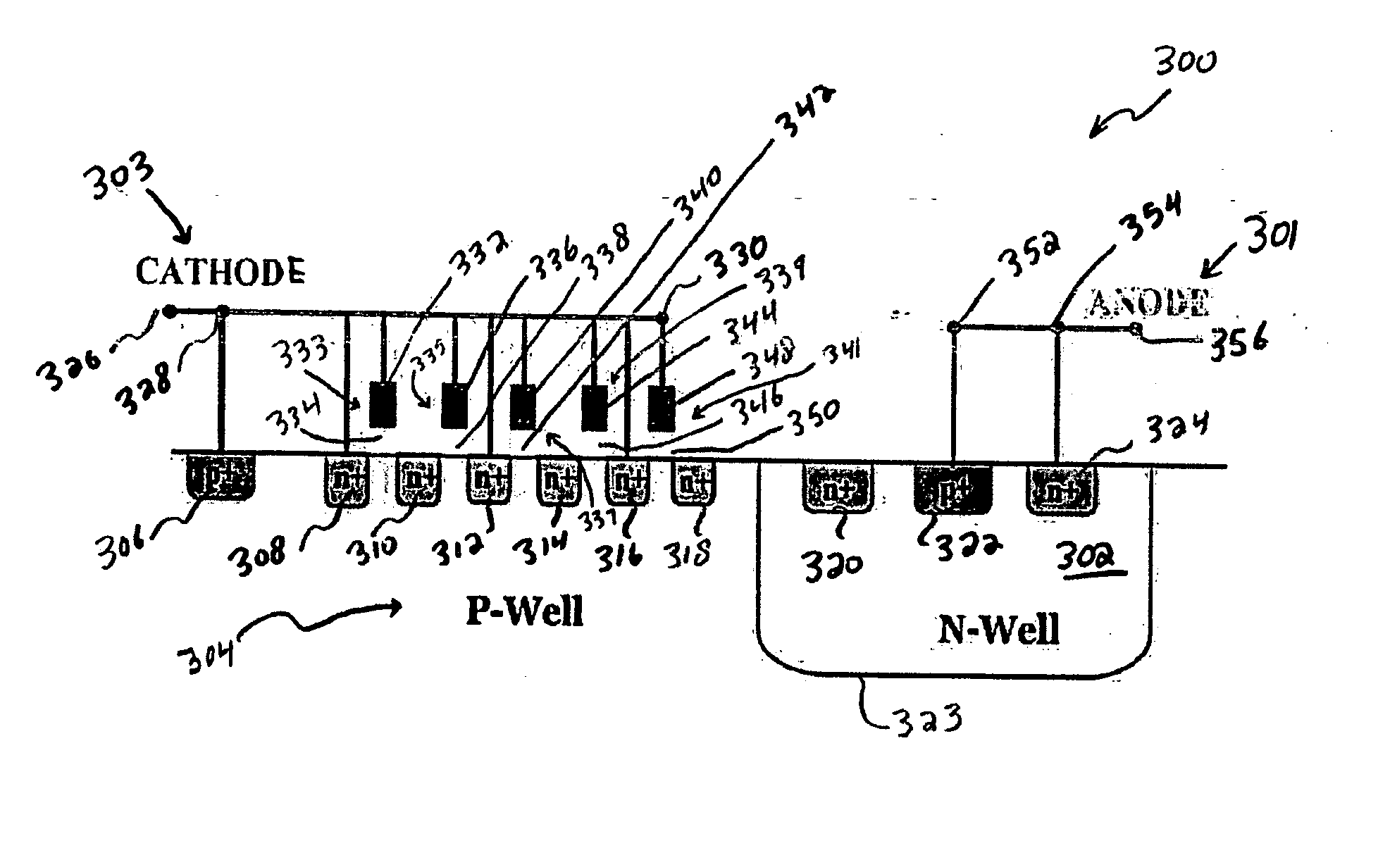
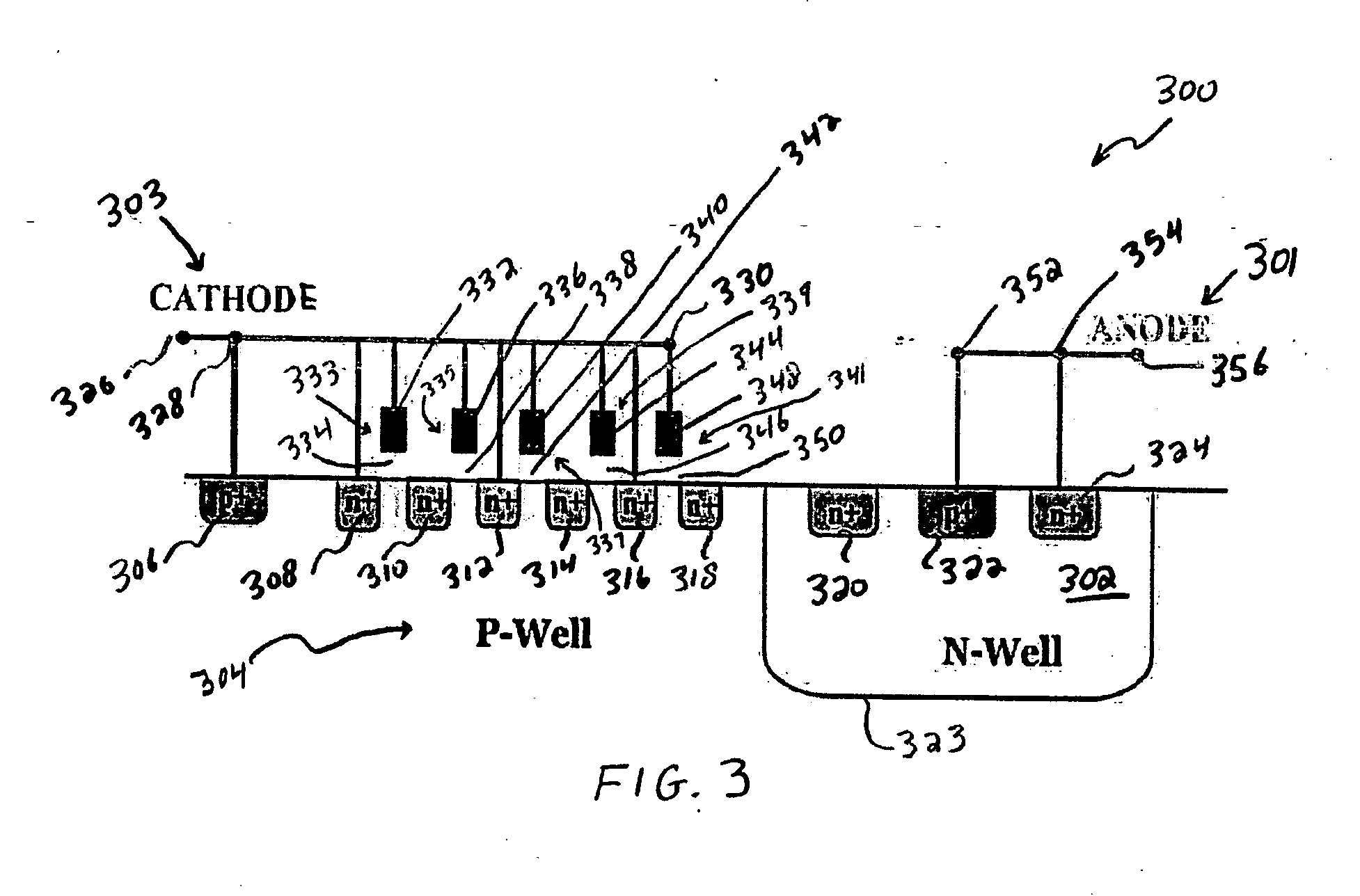
[0026]FIG. 3 illustrates a cross-sectional diagram of a low voltage triggered silicon-controlled rectifier (LVTSCR) apparatus 300 in which a plurality of NMOS fingers 333, 335, 337, 339, and 341 are incorporated therein, in accordance with a preferred embodiment. In order to improve the performance of an LVTSCR without scarifying HBM performance thereof, LVTSCR apparatus 300 can be inserted with multiple NMOS fingers 333, 335, 337, 339, and 341. Such an improvement can be verified, for example, utilizing 0.25 μm technology by utilizing a transmission line pulse generator (TLP). Note that as utilized herein, the acronym NMOS refers generally to “N-Channel Metal Oxide Semiconductor,” which is based on a transistor technology wherein the primary current carriers are...


PUM


Abstract

A silicon-controlled rectifier apparatus, comprising a substrate upon which a low-voltage triggered silicon-controlled rectifier is configured. A plurality of triggering components (e.g., NMOS fingers) are formed upon the substrate and integrated with the low-voltage triggered silicon-controlled rectifier, wherein the plurality of triggering components are inserted into the low-voltage triggered silicon-controlled rectifier in order to permit the low-voltage triggered silicon-controlled rectifier to protect against electrostatic discharge during human-body model and charged-device model stress events.

Description

TECHNICAL FIELD [0001] Embodiments are generally related to semiconductor devices. Embodiments are also related to silicon-controlled rectifier (SCR) devices utilized for electrostatic discharge (ESD) protection. Embodiments also relate to low-voltage triggered silicon-controlled rectifier devices. Embodiments are additionally related to human-body model (HBM) and charged-device model (CDM) devices and components. BACKGROUND OF THE INVENTION [0002] Silicon-controlled rectifiers (SCR) are utilized extensively in power device applications because of the capability to switch from a very high impedance state to a very low impedance state. For the same reason, a properly designed SCR can also be a very efficient electrostatic discharge (ESD) protection device. [0003] A semiconductor integrated circuit (IC) is generally susceptible to an electrostatic discharge (ESD) event that may damage or destroy the IC. An ESD event refers to a phenomenon of electrical discharge of a current (positive...

Claims


Application Information

Patent Timeline
IPC IPC(8): H01L29/74
CPCH01L29/87H01L27/0262
Inventor CHEN, JAU-WEN
Owner ORTIZ & LOPEZ PLLC
Why Eureka
Try Eureka