Intermediate connector for a tandem OLED device

a technology of tandem oled and connector, which is applied in the direction of thermoelectric devices, discharge tube luminescnet screens, natural mineral layered products, etc., can solve the problems of increased drive voltage, limited voltage available, short life, etc., and achieves lower operating voltage, lower voltage, and better stability

Inactive Publication Date: 2007-03-01
EASTMAN KODAK CO
View PDF6 Cites 114 Cited by
  • Summary
  • Abstract
  • Description
  • Claims
  • Application Information

AI Technical Summary

Benefits of technology

[0018] It is an advantage of this invention that it provides an OLED device that has better stability and operates at a lower voltage. It is a further advantage of this i

Problems solved by technology

In order to achieve high brightness, an OLED has to be operated at a relatively high current density, but this will result in a short lifetime.
Although tandem OLEDs have many advantages, one disadvantage is the increased drive voltage.
In many el

Method used


Image

  • Intermediate connector for a tandem OLED device
  • Intermediate connector for a tandem OLED device
  • Intermediate connector for a tandem OLED device

Examples


example 2 (

Inventive)

[0186] An inventive OLED device was constructed as in Example 1, except that in steps 7 and 13 the layer was a 50:50 mixture of Alq and Compound C-8 doped with 2% lithium metal.

examples 1-2

Results (Examples 1-2)

[0187] The devices were tested by applying a current across the electrodes of 20 mA / cm2 and measuring the spectrum and required drive voltage. The relative luminous efficiency is defined as the luminous efficiency of the example device, in cd / A, divided by the luminous efficiency in, cd / A, of reference Example 1. The CIE change magnitude is the magnitude of the color change in CIE color space relative to reference Example 1. The following table shows the results.

TABLE 1Example12Type (Inventive or Comparative)CompInvDrive voltage at 20 mA / cm211.710.5Relative Drive voltage1.000.90Yield (cd / A)17.317Relative Luminous Efficiency1.000.98CIE x0.310.32CIE y0.330.34CIE change magnitude—0.01

LUMO Values.

[0188] An important relationship exists when selecting the first compound(s) and second compound(s) of the invention. A comparison of the LUMO values of the first and second compounds in the layer of the invention, must be carefully considered. In devices of the invent...


PUM

PropertyMeasurementUnit
Timeaaaaaaaaaa
Percent by volumeaaaaaaaaaa

Abstract

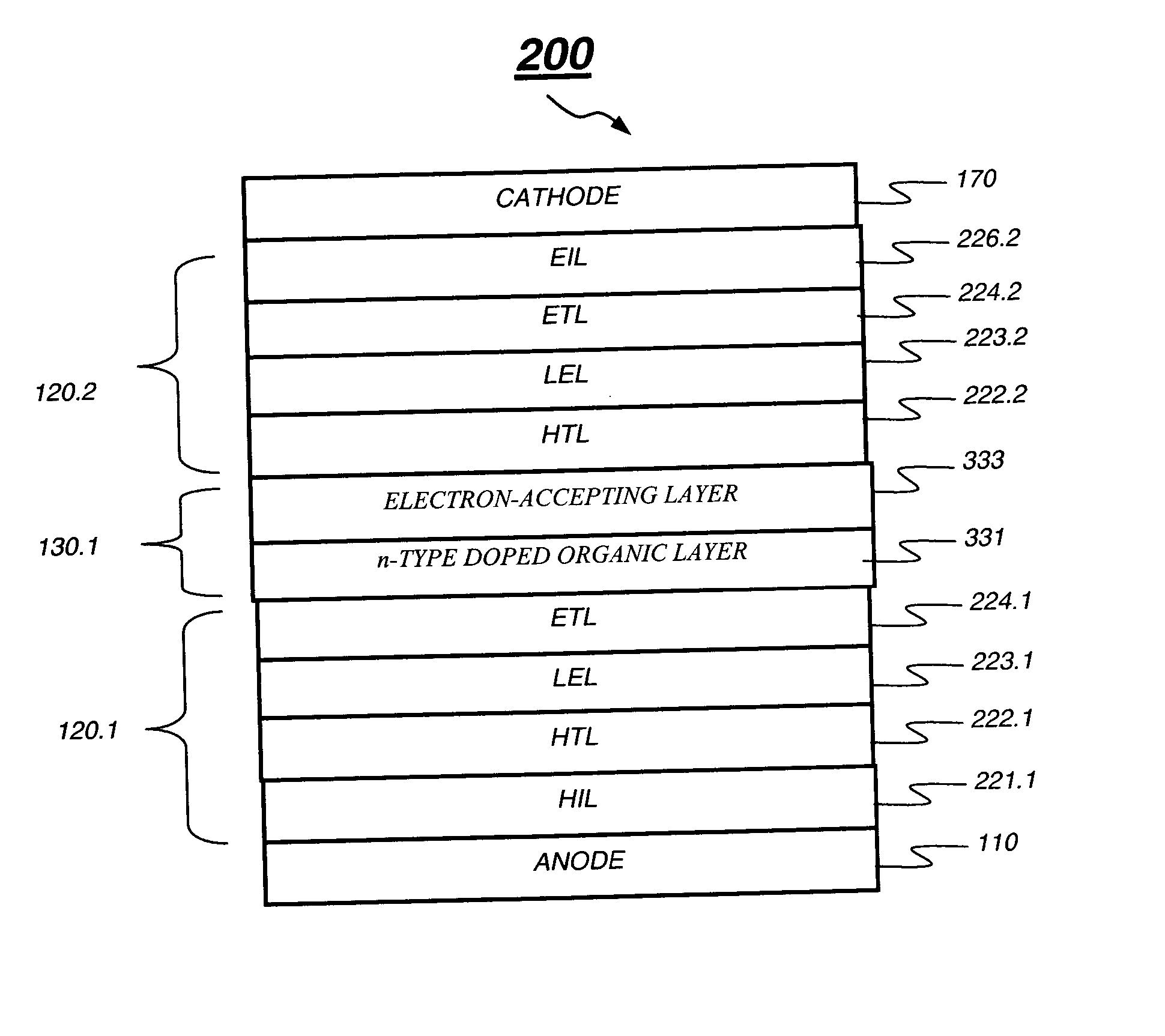
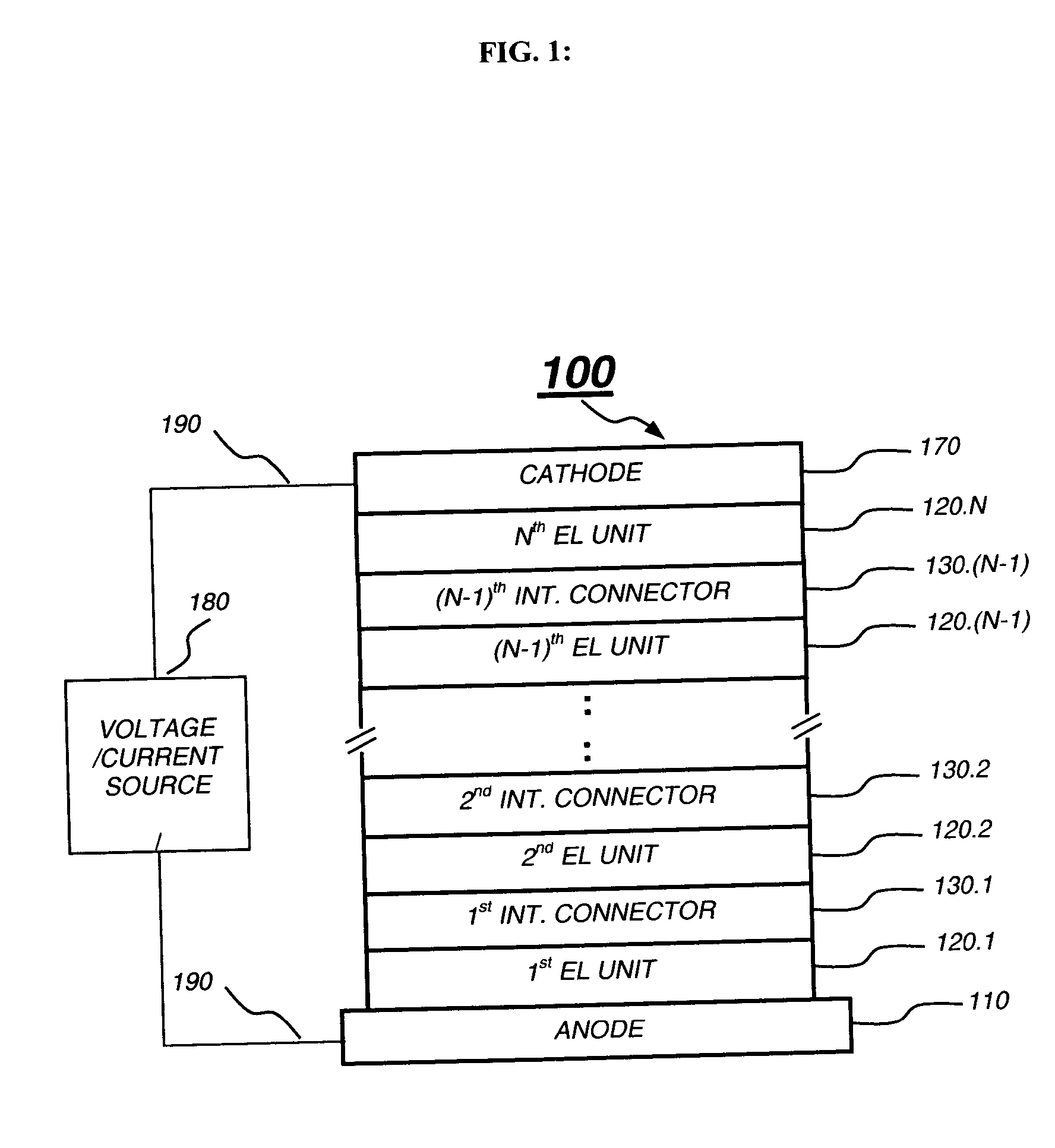
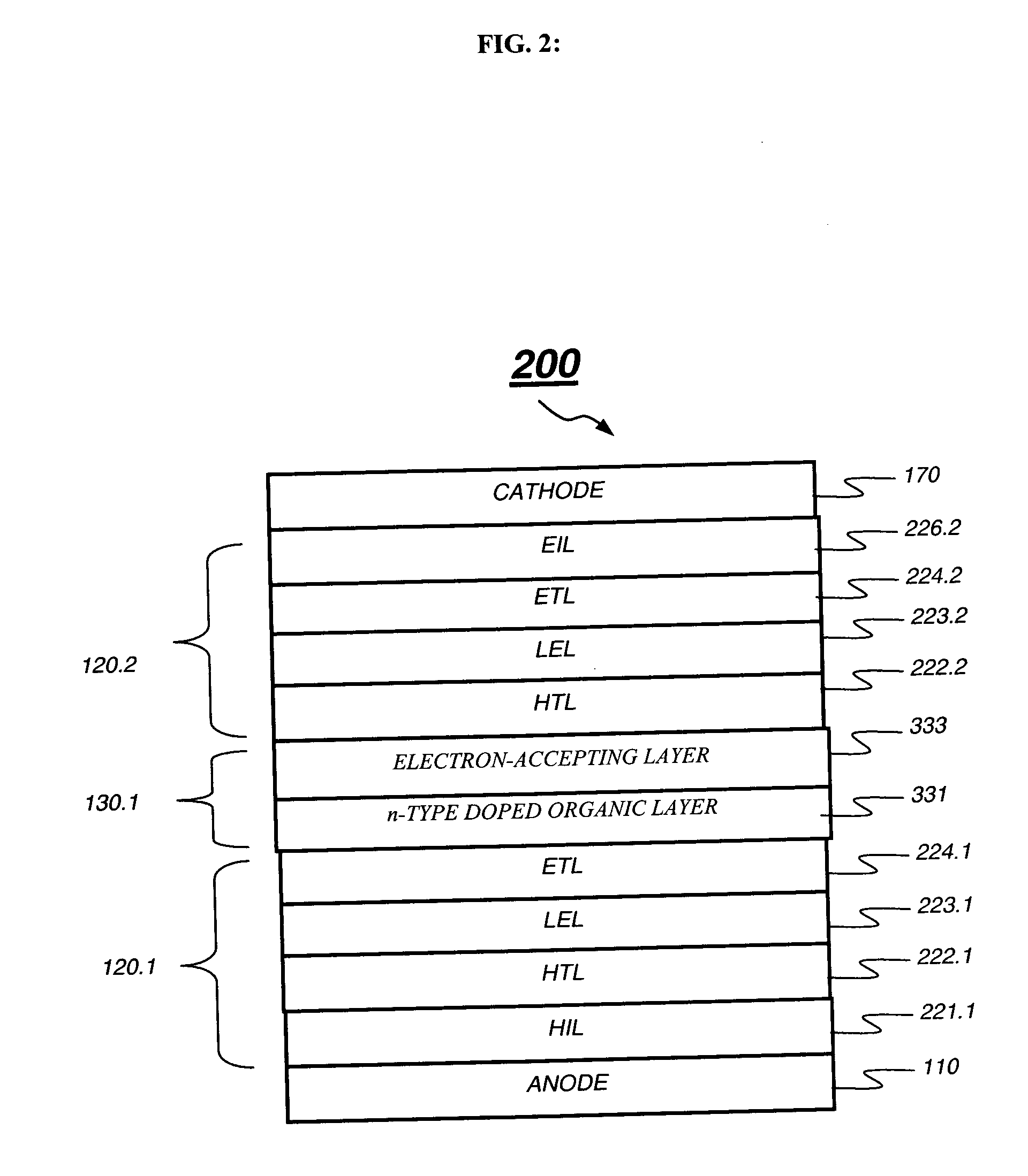
A tandem OLED device includes an anode, a cathode, at least first and second electroluminescent units disposed between the anode and the cathode. The electroluminescent units include an individually selected organic light-emitting layer and an intermediate connector disposed between the first and second electroluminescent units. The intermediate connector includes an n-type doped organic layer having an n-type dopant and an electron-transporting material. The electron-transporting material is a mixture of a first organic compound that has the lowest LUMO value of the compounds in the n-type doped organic layer, in an amount greater than or equal to 10% by volume and less than 100% by volume of the layer; at least one second organic compound exhibiting a higher LUMO value than the first organic compound.

Description

CROSS REFERENCE TO RELATED APPLICATIONS [0001] Reference is made to commonly assigned U.S. patent application Ser. No. 11 / 077,218, filed Mar. 10, 2005 by Begley et al., entitled “Organic Light-Emitting Devices With Mixed Electron Transport Materials”; U.S. patent application Ser. No. 11 / 110,071, filed Apr. 20, 2005 by Hatwar et al., entitled “Tandem OLED Device”; and U.S. patent application Ser. No. ______, filed concurrently herewith, by Hatwar et al., entitled “Electron-Transporting Layer for White OLED Device” the disclosures of which are incorporated herein by reference.FIELD OF THE INVENTION [0002] The present invention relates to tandem OLED devices, and more particularly, to an intermediate connector for use in such devices. BACKGROUND OF THE INVENTION [0003] Organic electroluminescent (EL) devices or organic light-emitting diodes (OLEDs) are electronic devices that emit light in response to an applied potential. The structure of an OLED includes, in sequence, an anode, an or...

Claims


Application Information

Patent Timeline
IPC IPC(8): H01L51/52H01L51/54
CPCH01L51/002H01L51/0054H01L51/5278H01L51/0081H01L51/5052H01L51/0058H10K71/30H10K85/622H10K85/626H10K85/324H10K50/165H10K50/19
Inventor HATWAR, TUKARAM K.BAGLEY, WILLIAM J.
Owner EASTMAN KODAK CO
Why Eureka
Try Eureka