

Plasmonic array for maskless lithography
a plasmonic array and maskless technology, applied in the field of photolithography apparatus and methods, can solve the problems of time-consuming and complex design and fabrication of masks
- Summary
- Abstract
- Description
- Claims
- Application Information
AI Technical Summary
Problems solved by technology
Method used
Image

Examples
Embodiment Construction
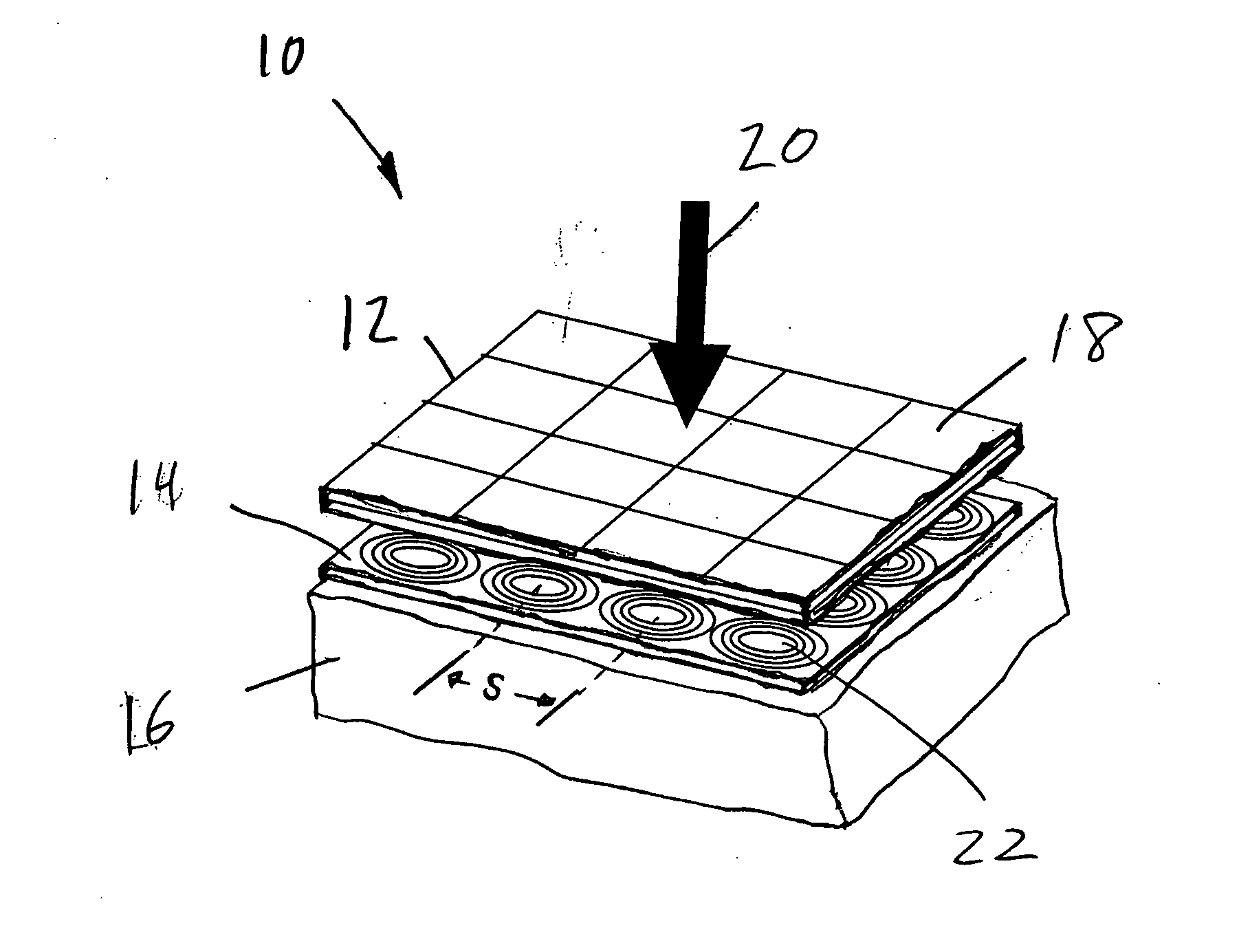
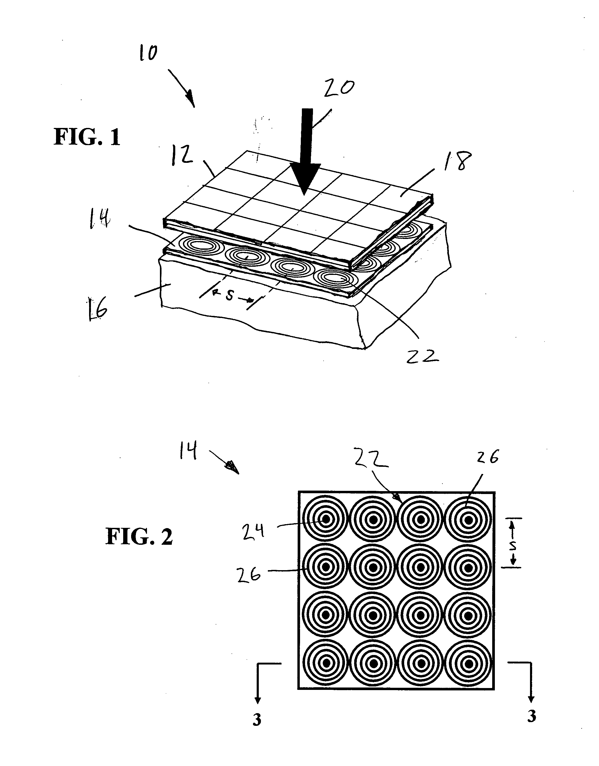
[0016]FIG. 1 shows an apparatus 10 comprising a spatial light modulator 12 and a plasmonic lens array 14 disposed over a semiconductor wafer 16. The spatial light modulator 12 comprises a plurality of pixels 18 each comprising at least one light modulator. Light, represented by arrow 20, propagates through the spatial light modulator 12. The pixels 18 can be selectively activated to control light propagation through the pixels. Spatial light patterns can thereby be formed. Examples of such spatial light modulators include liquid crystal spatial light modulators and faraday rotators, although the type of spatial light modulator is not limited to those described herein as other types of spatial light modulator devices both well known in the art and yet to be devised may be used.
[0017] The plasmonic lens array 14 comprises a plurality of plasmonic lenses 22 that focus light propagated through the spatial light modulator 12 onto the semiconductor wafer 16. The plasmonic lenses 22 are s...
PUM
| Property | Measurement | Unit |
|---|---|---|
| width | aaaaa | aaaaa |
| width | aaaaa | aaaaa |
| distance | aaaaa | aaaaa |
Abstract
Description
Claims
Application Information