Semiconductor device and method for manufacturing the same
a technology of semiconductor devices and films, applied in the direction of semiconductor devices, basic electric elements, electrical appliances, etc., can solve the problems of difficult to form only films having a high relative permittivity, and the original object of increasing the capacity cannot be achieved, so as to achieve good fet quality and improve the quality of the interfacial surface
- Summary
- Abstract
- Description
- Claims
- Application Information
AI Technical Summary
Benefits of technology
Problems solved by technology
Method used
Image
Examples
first embodiment
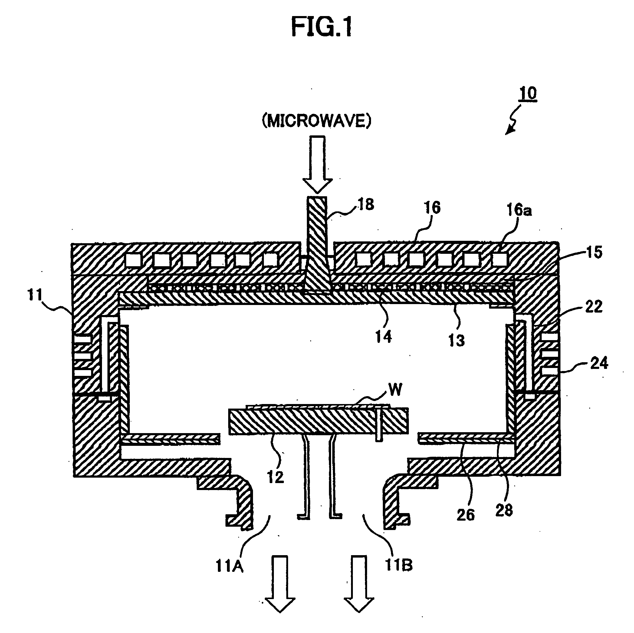
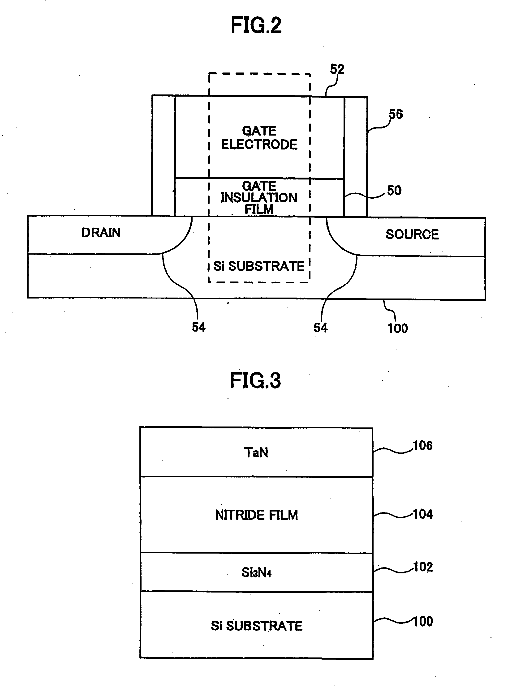
[0030]FIG. 3 is a schematic diagram showing the configuration of the substantial part of the semiconductor device according to the present invention. In the semiconductor device of the present embodiment, a nitride High-K film 104 is formed as a gate insulation film (50) on the silicon substrate 100. A silicon nitride film (Si3N4 layer) 102 is formed between the silicon substrate 100 and the High-K film 104. Further, a TaN layer 106 is formed as a gate electrode (52) on the High-K film 104 by spattering. The High-K film 104 is formed by using the plasma treatment device 10 according to a plasma CVD technology. The silicon nitride film 102 is formed in the same way by using the plasma treatment apparatus 10 according to a direct radical nitriding treatment. The silicon nitride film 102 performs a function of lowering the interface state.
[0031] As the High-K film 104, for example, one of the following compositions can be adopted:
M3Si6N11(M = La, Ce, Pr, Nd, Sm);M2Si5N8(M = Ca, Sr, B...
third embodiment
[0036]FIG. 5 is a schematic diagram showing the configuration of the substantial part of the semiconductor device according to the present invention. In FIG. 5, the same or the corresponding components of FIG. 3 and FIG. 4 are allocated the same reference numbers, and overlapping descriptions are omitted. In the configuration of the present embodiment, the High-K film 104 is formed between the silicon substrate 100 and the gate electrode layer (TaN layer); however, another layer such as a Si3N4 layer is not formed between the silicon substrate 100 and the High-K film 104 or between the High-K film 104 and the TaN layer 106.
fourth embodiment
[0037]FIG. 6 is a schematic diagram showing the configuration of the substantial part of the semiconductor device according to the present invention. In FIG. 6, the same or the corresponding components of FIG. 3 through FIG. 5 are allocated the same reference numbers, and overlapping descriptions are omitted. In the configuration of the present embodiment, a buffer layer 110 is formed between the silicon substrate 100 and the High-K film 104. It should be noted, however, that another layer such as a Si3N4 layer is not provided between the High-K film 104 and the TaN layer 106.
[0038] The buffer layer 110 is formed by changing the composition of the gas which is supplied to the treatment container 11 in the same process of forming the High-K film 104. The buffer layer 110 has the benefit of a relative permittivity higher than that of the Si3N4 layer, and an interface state which can be lowered.
PUM
 Abstract
Description
Claims
Application Information


