Vertical LC tank device

Inactive Publication Date: 2007-03-08
IBM CORP
View PDF12 Cites 61 Cited by
  • Summary
  • Abstract
  • Description
  • Claims
  • Application Information

AI Technical Summary

Problems solved by technology

Thus large regions of prime chip area are effectively wasted and the parasitic capacitances of the long metal connections over the

Method used


Image

  • Vertical LC tank device
  • Vertical LC tank device
  • Vertical LC tank device

Examples


first embodiment

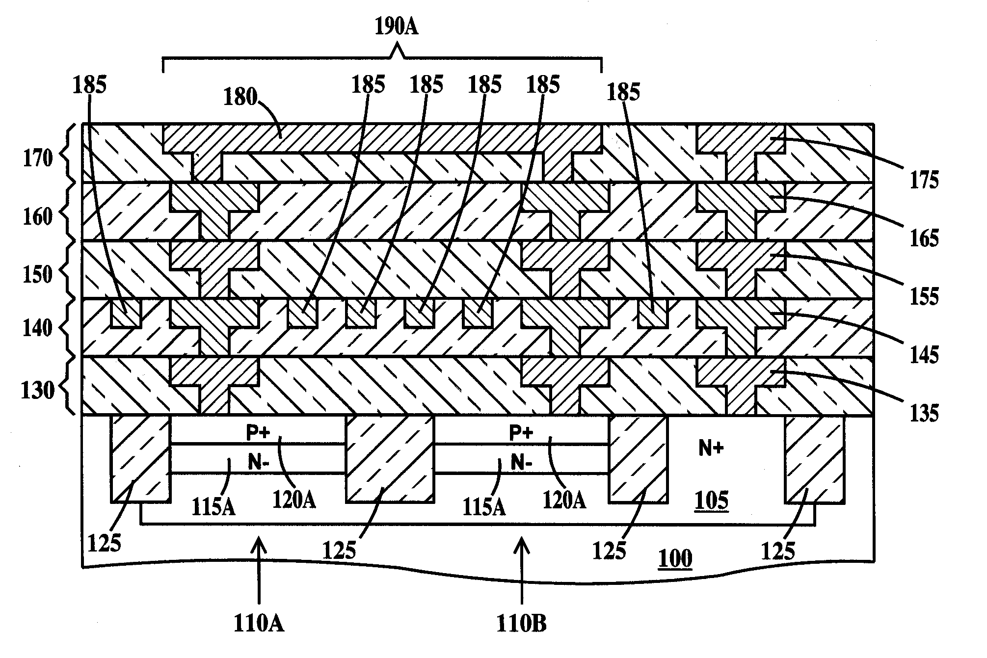
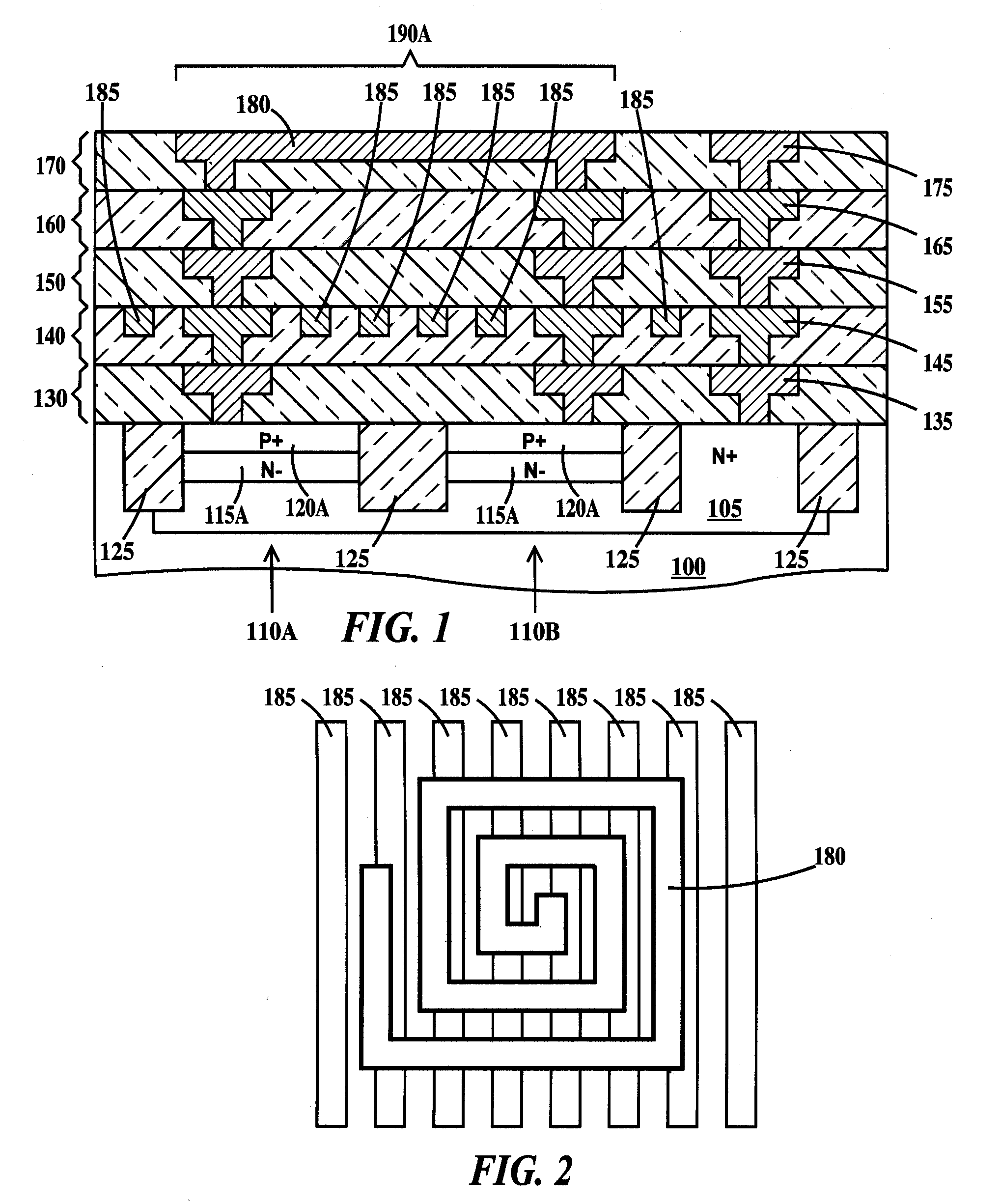
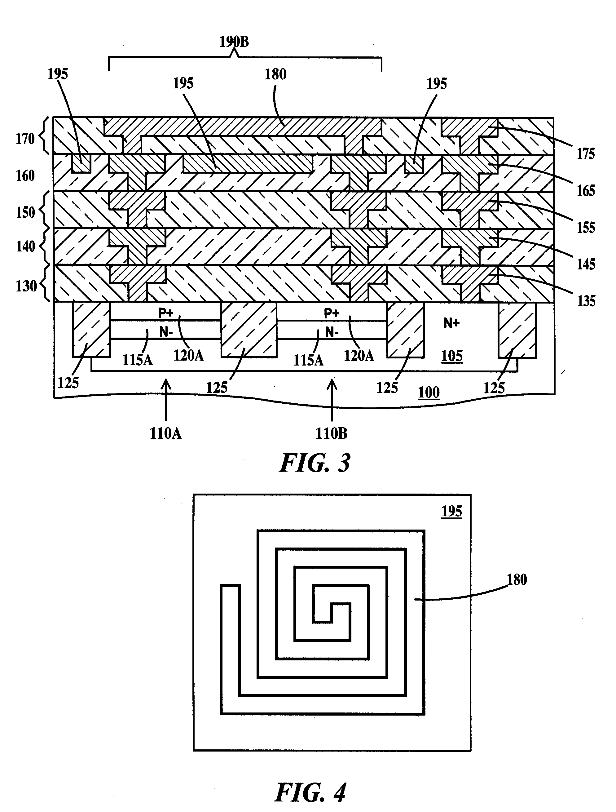
[0018]FIG. 1 is a cross-sectional view of an LC tank device according to the present invention. Formed in a silicon substrate 100 (or a silicon layer on a silicon-on insulator (SOI) substrate) is an N-well region 105. Formed in N-well region 105 are varactors 110A and 110B. Varactor 110A comprises a lightly doped N-type region 115A between a highly doped P region 120A and the highly doped N-well 105. Varactor 110B comprises a lightly doped N-type region 115B between a highly doped P region 120B and the highly doped N-well 105. Regions 115A and 115B as well as regions 120A and 120B are isolated from each other by shallow trench isolation (STI) 125. Varactors 110A and 110B are examples of a typical p-n junction based varactor diode. Varactors 110A and 110B may be replaced with other varactor types such as hyper abrupt junction (HAVAR) varactors, MOS varactors (see FIG. 12).

[0019] Formed a top surface of substrate 105 is a first dielectric layer 130 which includes conductive metal vias...

second embodiment

[0024]FIG. 3 is a cross-sectional view of an LC tank device according to the present invention. FIG. 3 is similar to FIG. 1 except an LC tank device 190B includes a magnetic shield 195 in place of patterned electric shield 185 of FIG. 1. Magnetic shield 195 is formed in fourth dielectric layer 160. Magnetic shield 195 is a solid plate except for through holes for vias 165 and is advantageously placed in a high wiring level (a wiring level near to inductor 180) in order to maximize the number of wiring levels where normal integrated circuit wires may pass under the shield.

[0025]FIG. 4 is a plan view of portions of the LC tank device according to the second embodiment of the present invention. In FIG. 4, it can be seen that inductor 180 has the shape of a spiral and magnetic shield 195 comprises a continuous region with no openings.

[0026] It should be noted, that varactors 110A and 110B are aligned within the perimeter defined by the outermost coils of inductor 180 and that magnetic ...

third embodiment

[0027]FIG. 5 is a cross-sectional view of an LC tank device according to the present invention. FIG. 5 is similar to FIG. 1 except an LC tank device 190C includes a magnetic core inductor 200A in place of inductor 180 of FIG. 1 Magnetic core inductor 200A comprises a loop coil conductor 205A between an inner magnetic core 205B, an outer magnetic loop 205C and a magnetic plate 205D under loop coil conductor 205A, magnetic core 205B and outer magnetic loop 205C and there is no patterned shield. Magnetic plate 205D includes through holes for vias 165. Magnetic core inductor 200A is formed in fourth and fifth dielectric layers 160 and 170. Magnetic core inductor 200A is advantageously placed in the highest wiring levels (the wiring levels furthest from substrate 100) in order to maximize the number of wiring levels where normal integrated circuit wires may pass under inductor 200A. Loop conductor 205A inner magnetic core 205B, outer magnetic loop 205C in fifth dielectric layer 170 are n...


PUM


Abstract

An LC tank structure. The structure, including a set of wiring levels on top of a semiconductor substrate, the wiring levels stacked on top of each other from a lowest wiring level nearest the substrate to a highest wiring level furthest from the substrate; an inductor in the highest wiring level, the inductor confined within a perimeter of a region of the highest wiring level; and a varactor formed in the substrate, the varactor aligned completely under the perimeter of the region of the highest wiring level. The structure may additionally include an electric shield in a wiring level of the set of wiring levels between the lowest wiring level and the highest wiring level. Alternatively, the inductor includes a magnetic core and alternating electrically non-magnetic conductive metal coils and magnetic coils around the core.

Description

FIELD OF THE INVENTION [0001] The present invention relates to the field of LC tank devices for integrated circuits; more specifically, it relates to an LC tank device comprising an inductor and varactor on an integrated circuit chip. BACKGROUND OF THE INVENTION [0002] Conventional LC tank devices require a protected area within which the inductor portion of the LC tank device is placed and the varactor portion of the LC tank device or any other devices of integrated circuits of integrated circuit chips are excluded in order to avoid, eddy currents and electric field coupling to elements of the integrated circuits. Thus large regions of prime chip area are effectively wasted and the parasitic capacitances of the long metal connections over the protection area between the inductor and the varactor reduce the quality (Q) value and the frequency tuning range of the LC tank. The horizontal metal connections dominate the total connection parasitic capacitances. In order to recover these ...

Claims


Application Information

Patent Timeline
IPC IPC(8): H01L29/00
CPCH01L23/5223H01L23/5225H01L23/5227H01L27/0617H01L27/0641H01L27/08H01L27/0811H01L2924/0002H01L28/10H03J3/20H03L7/099H01L2924/00
Inventor DING, HANYIFENG, KAI D.HE, ZHONG-XIANGLIU, XUEFENG
Owner IBM CORP
Why Eureka
Try Eureka