Partitioning of radio-frequency apparatus

a radio-frequency apparatus and circuit technology, applied in the field of circuit partitioning of radio-frequency apparatus, can solve the problems of reducing the interference effect of the various circuitry blocks of the transceiver, and no technology for addressing all of the above problems in high-performance rf receivers or transceivers, etc., and achieves the effect of reducing the interference effect among the circuit partitions and reducing the interference effect among the three circuit partitions

Inactive Publication Date: 2007-03-08
SILICON LAB INC
View PDF99 Cites 53 Cited by
  • Summary
  • Abstract
  • Description
  • Claims
  • Application Information

AI Technical Summary

Benefits of technology

[0093] The embodiment 200A in FIG. 2A comprises a first circuit partition, or circuit block, 214 that includes the receiver analog circuitry 208 and the transmitter circuitry 216. The embodiment 200A also includes a second circuit partition, or circuit block, that includes the receiver digital circuitry 212. The embodiment 200A further includes a third circuit partition, or circuit block, that comprises the local oscillator circuitry 222. The first circuit partition 214, the second circuit partition 212, and the third circuit partition 222 are partitioned from one another so that interference effects among the circuit partitions tend to be reduced. The first, second, and third circuit partitions preferably each reside within an integrated circuit device. In other words, preferably the receiver analog circuitry 208 and the transmitter circuitry 216 reside within an integrated circuit device, the receiver digital circuitry 212 re...

Problems solved by technology

From the perspective of the transceiver's circuitry, RF transceivers typically include sensitive components susceptible to noise and interference with one another and with external sources.
Integrating the transceiver's circuitry into one integrated circuit may exacerbate interference among the various blocks of the transceiver's circuitry.
Unfortunately, no technique for addressing all of the above issues in high-performance RF receivers or transceivers, for example, RF transceivers used in cellular and telephony applications, has been developed.
Furthermore, discrete components increase the overall system cost, complexity, power consumption, and form factor (e.g., board size, number of package pins).
Worse yet, discrete components reduce the system's overall integration level, reliability, and speed or throughput.
In addition, conventional discrete VCOs typic...

Method used


Image

  • Partitioning of radio-frequency apparatus
  • Partitioning of radio-frequency apparatus
  • Partitioning of radio-frequency apparatus

Examples


embodiment 400

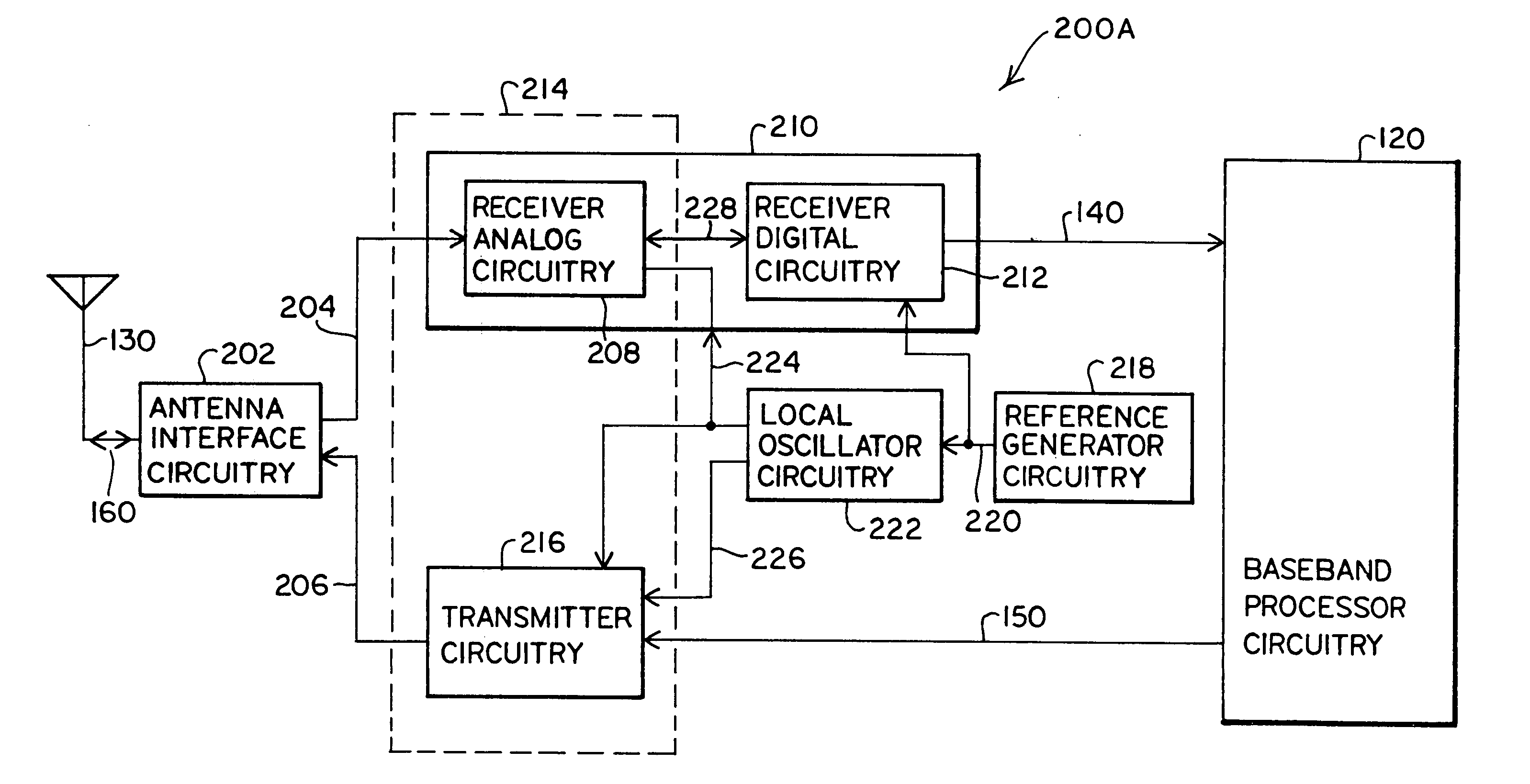
[0105]FIG. 4 shows a more detailed block diagram of an embodiment 400 of an RF transceiver partitioned according to the invention. The transceiver includes receiver analog circuitry 408, receiver digital circuitry 426, and transmitter circuitry 465. In the receive mode, the antenna interface circuitry 202 provides an RF signal 401 to a filter circuitry 403. The filter circuitry 403 provides a filtered RF signal 406 to the receiver analog circuitry 408. The receiver analog circuitry 408 includes down-converter (i.e., mixer) circuitry 409 and analog-to-digital converter (ADC) circuitry 418. The down-converter circuitry 409 mixes the filtered RF signal 406 with an RF local oscillator signal 454, received from the local oscillator circuitry 222. The down-converter circuitry 409 provides an in-phase analog down-converted signal 412 (i.e., I-channel signal) and a quadrature analog down-converted signal 415 (i.e., Q-channel signal) to the ADC circuitry 418.

[0106] The ADC circuitry 418 conv...

embodiment 700

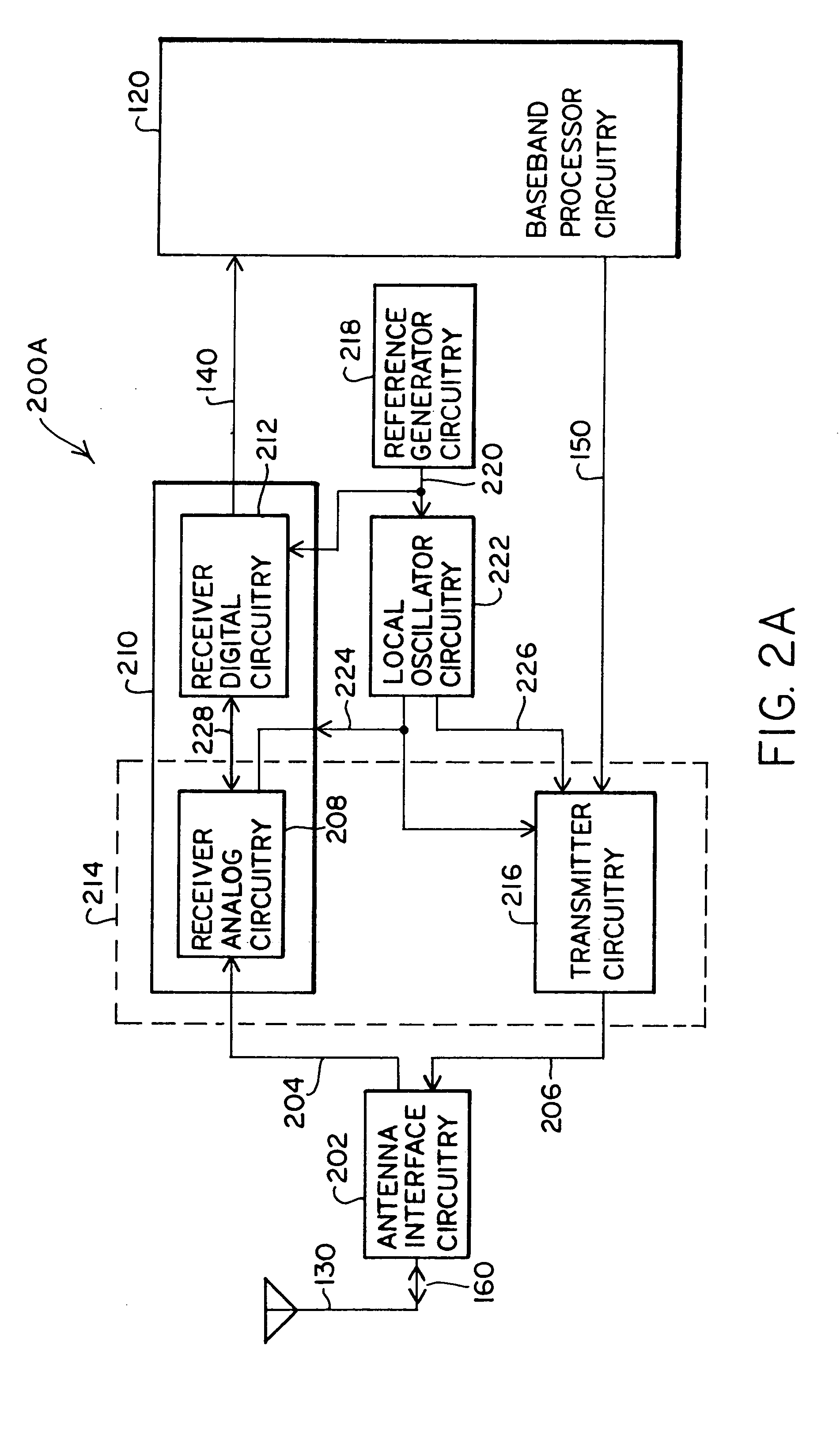
[0125] Because the embodiment 700 includes the function of the receiver digital circuitry 426 within the baseband processor circuitry 120, it includes two circuit partitions, or circuit blocks. A first circuit partition 710 includes the receiver analog circuitry 408 and the transmitter circuitry 465. A second circuit partition comprises the local oscillator circuitry 222. Note also that, similar to the RF transceiver shown in FIG. 2C, one may also include within the baseband processor circuitry 120 the functionality of the reference generator circuitry 218, as desired.

[0126]FIG. 8 shows an embodiment 800 of a multi-band RF transceiver, partitioned according to the invention. Preferably, the RF transceiver in FIG. 8 operates within the GSM (925 to 960 MHz for reception and 880-915 MHz for transmission), PCS (1930 to 1990 MHz for reception and 1850-1910 MHz for transmission), and DCS (1805 to 1880 MHz for reception and 1710-1785 MHz for transmission) bands. Like the RF transceiver in ...

embodiment 800

[0145] Like the transceiver in FIG. 4, if the receiver digital circuitry 851 need not be compatible with the common analog interface to baseband processors, one may remove the DAC circuitry 875A and 875B, and use a digital interface to the baseband processor circuitry 120, as desired. In fact, similar to the RF transceiver shown in FIG. 2D, one may realize the function of the receiver digital circuitry 851 within the baseband processor circuitry 120, using hardware, software, or a combination of hardware and software. In that case, the RF transceiver would include two circuit partitions, or circuit blocks. The first circuit partition 801 would include the receiver analog circuitry 839 and the transmitter circuitry 877. A second circuit partition would comprise the local oscillator circuitry 222. Note also that, similar to the RF transceiver shown in FIG. 2C, in the embodiment 800, one may include within the baseband processor circuitry 120 the functionality of the reference generato...


PUM


Abstract

Components of a radio-frequency (RF) apparatus including transceiver circuitry and frequency modification circuitry of a crystal oscillator circuit that generates a reference signal with adjustable frequency may be partitioned in a variety of ways, for example, as one or more separate integrated circuits. The frequency modification circuitry may be implemented as part of a crystal oscillator circuit that includes digitally controlled crystal oscillator (“DCXO”) circuitry and a crystal. The frequency modification circuitry may include at least one variable capacitance device and may be employed to generate a reference signal with adjustable frequency. The adjustable reference signal may be provided to other components of the RF apparatus and/or the RF apparatus may be configured to provide the adjustable reference signal to baseband processor circuitry. Automatic frequency control (AFC) circuitry may be integrated with other components of RF circuitry and may generate frequency control signals for the frequency modification circuitry based on, for example, a signal received from a temperature sensor. Digital-to-analog converter (DAC) circuitry may be integrated with other components of RF circuitry to enable all-digital frequency control communications from baseband processor circuitry to RF circuitry.

Description

CROSS-REFERENCE TO RELATED APPLICATIONS [0001] This patent application is a continuation-in-part of U.S. patent application Ser. No. 10 / 075,094, Attorney Docket No. SILA:074, titled “Radio-Frequency Communication Apparatus And Associated Methods,” filed on Feb. 13, 2002; which is incorporated herein by reference. This patent application also claims priority from U.S. Provisional Patent Application Ser. No. 60 / 405,959, Attorney Docket No. SILA:127PZ1, titled “Integrated Controlled Crystal Oscillator In Radio-Frequency Apparatus And Associated Methods,” filed on Aug. 26, 2002, which is incorporated herein by reference. This patent application also claims priority from U.S. Provisional Patent Application Ser. No. 60 / 399,988, Attorney Docket No. SILA:123PZ1, titled “Digitally Calibrated Crystal Oscillator In Radio-Frequency Communication Apparatus And Associated Methods,” filed on Jul. 31, 2002, which is incorporated herein by reference. [0002] The aforementioned U.S. patent application...

Claims


Application Information

Patent Timeline
IPC IPC(8): H04B1/38
CPCH03J2200/10H04L27/0002H04B1/30
Inventor MALIGEORGOS, JAMESMARQUES, AUGUSTO M.LIM, LYSANDERTUTTLE, G. TYSONRAFI, ASLAMALI A.PAULUS, TODUEHARA, GREGORY T.SCOTT, JEFFREY W.BEHRENS, RICHARD T.KERTH, DONALD A.VISHAKHADATTA, G. DIWAKARSRINIVASAN, VISHNU S.WANG, CAIYI
Owner SILICON LAB INC
Why Eureka
Try Eureka