Coating and developing apparatus

a technology of developing apparatus and coating, which is applied in the direction of coatings, instruments, photosensitive materials, etc., can solve the problems of difficult maintenance of the apparatus, difficult to arrange an effective transfer schedule, and difficult to transport the coating and developing apparatus. achieve the effect of reducing height and length and high transferring efficiency in the apparatus

Active Publication Date: 2007-03-15
TOKYO ELECTRON LTD
View PDF3 Cites 54 Cited by
  • Summary
  • Abstract
  • Description
  • Claims
  • Application Information

AI Technical Summary

Benefits of technology

[0009] The present invention has been made under the foregoing circumstances, and it is therefore an object of the present invention to provide a coating and developing apparatus that achieves reduction in height and length thereof to a reasonable degree while achieving high transferring efficiency in the apparatus.

Problems solved by technology

In the coating and developing apparatus of JP2004-193597A, since a common transfer means transfers a wafer to units for processing a wafer before exposure (e.g., a unit for resist film formation) and also transfers a wafer to units for processing a wafer after exposure (e.g., a developing unit), it is difficult to arrange an effective transferring schedule and thus to improve the throughput.
Thus, it is difficult to transport the coating and developing apparatus from the manufacturing maker of the apparatus to the user.
Moreover, the maintenance of the apparatus is difficult.
On the contrary, if liquid processing units such as a resist film coating unit and an antireflective film forming units are arranged in a plane, the footprint of the apparatus drastically increases.

Method used


Image

  • Coating and developing apparatus
  • Coating and developing apparatus
  • Coating and developing apparatus

Examples


first embodiment

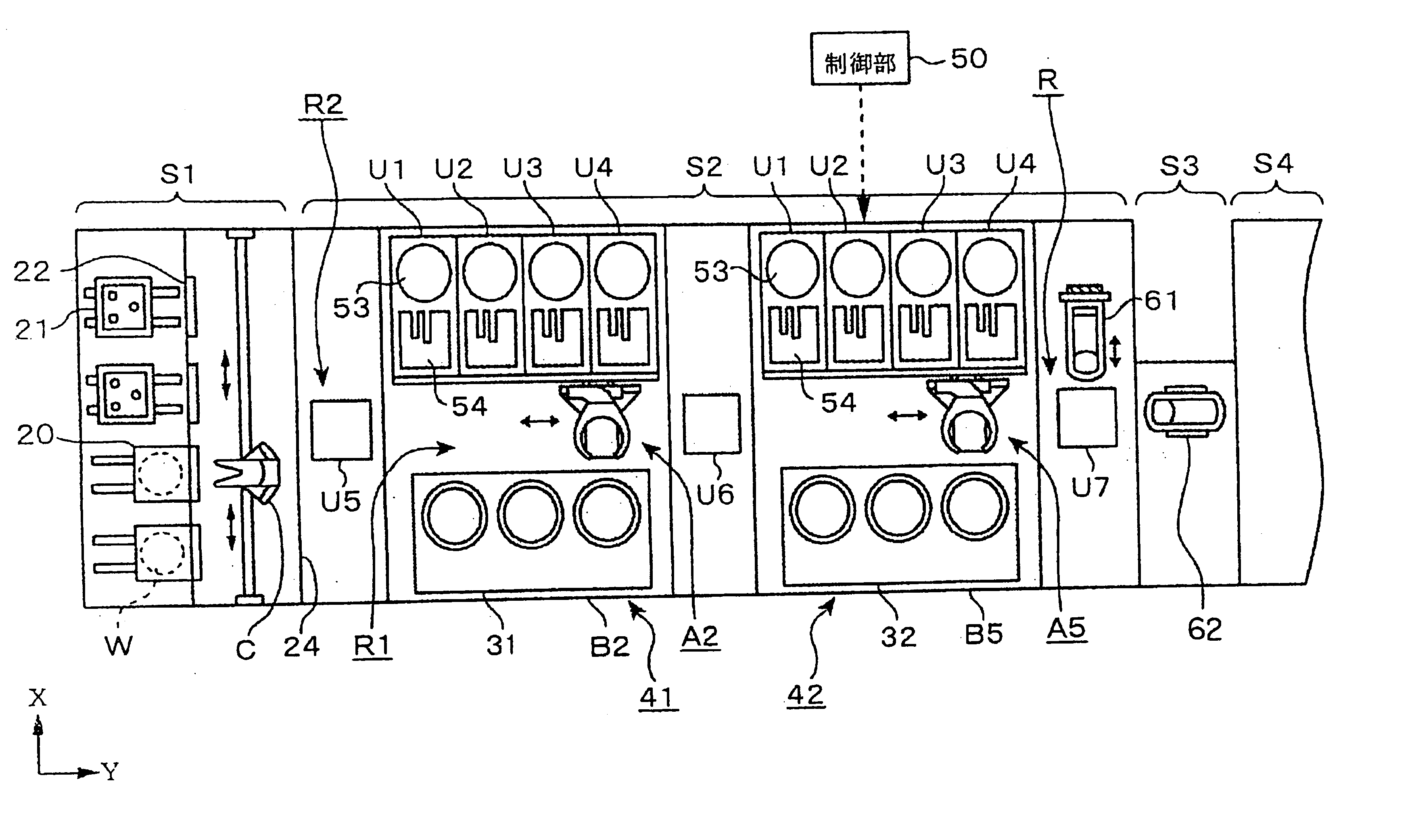
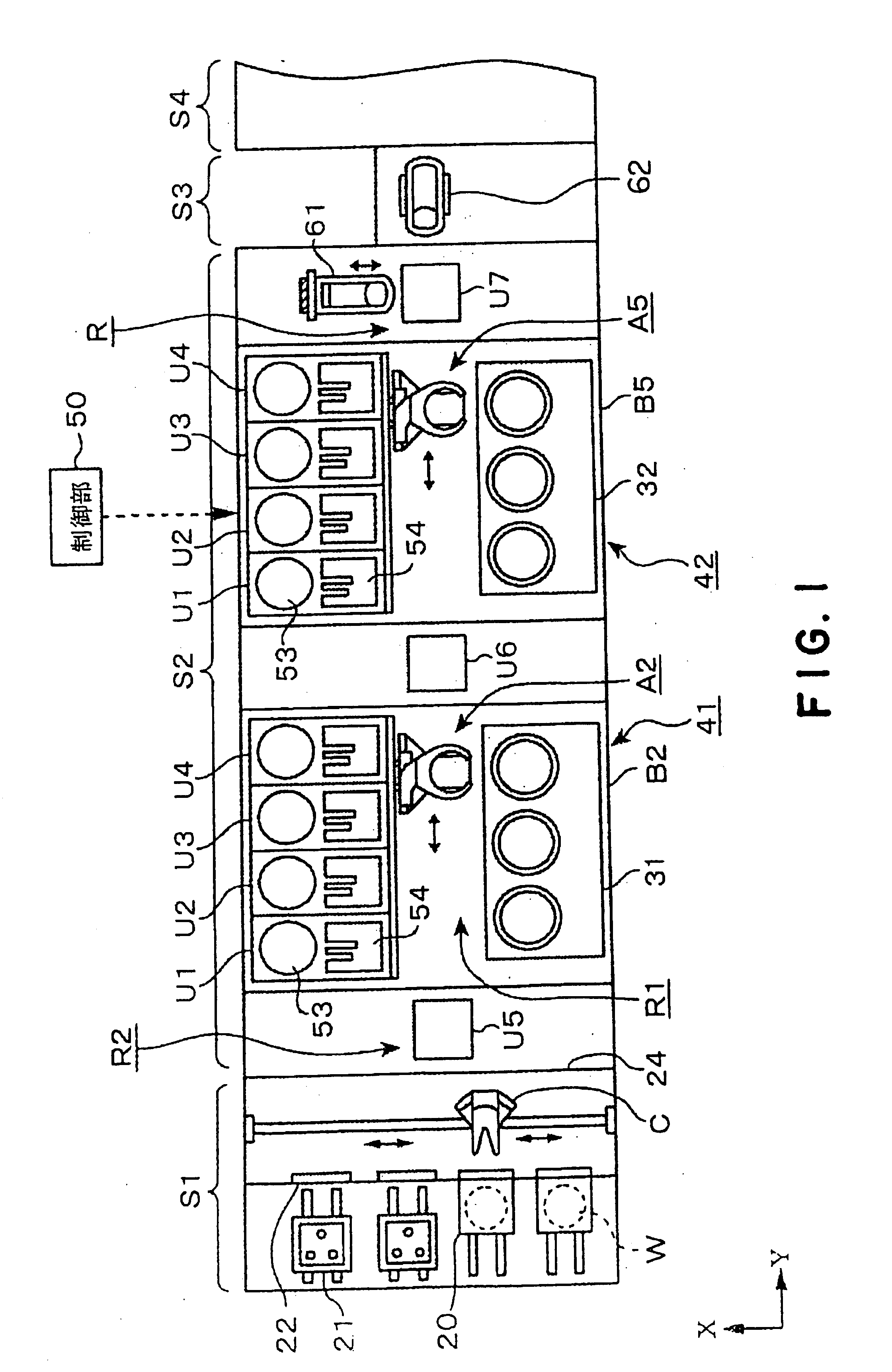
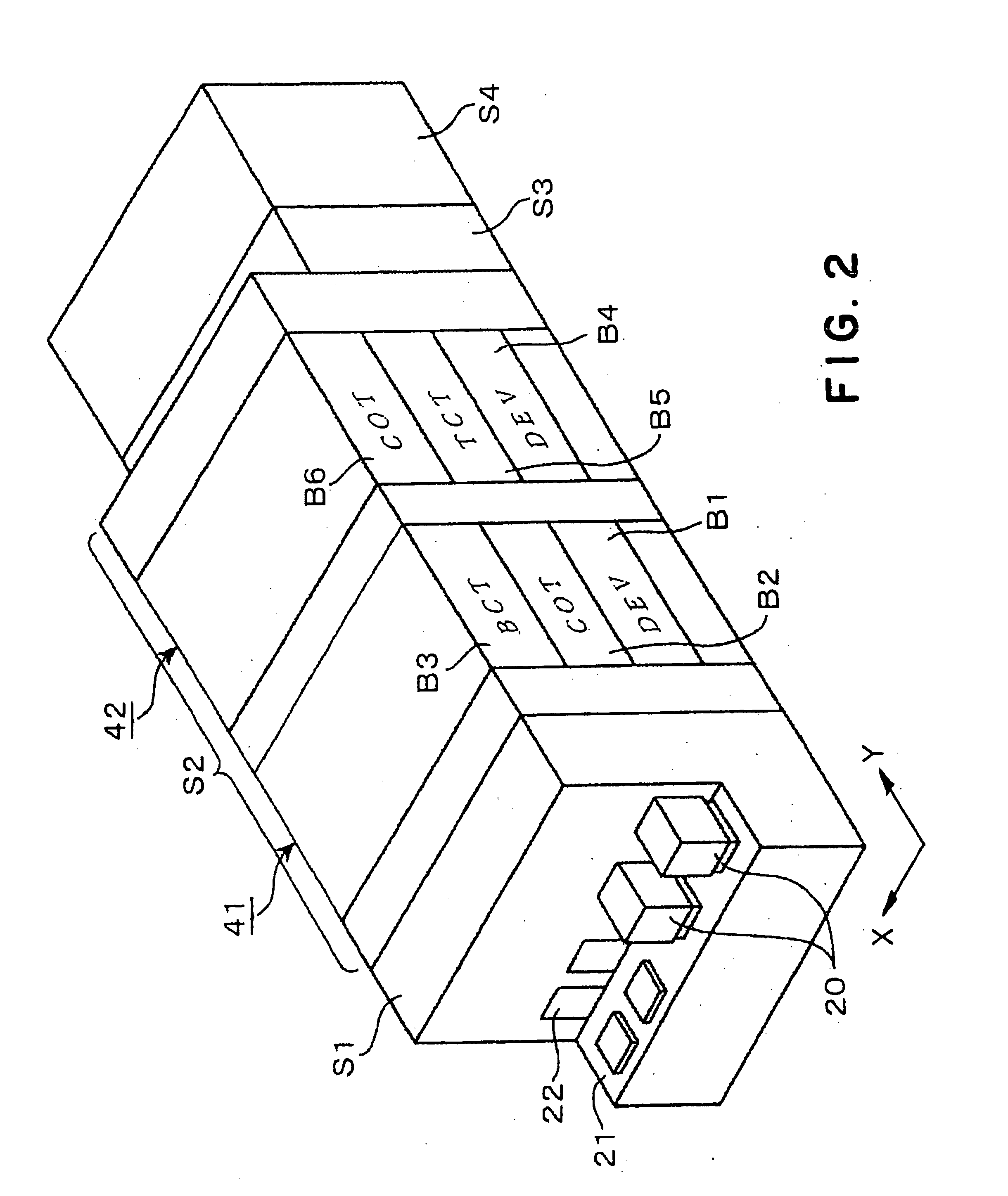
[0088] In the foregoing (a) the processing units relating to a liquid process and the transfer means are integrated to form a unit block; (b) the unit blocks relating to pre-exposure coating processes (the COT layers B2 and B6, the BCT layer B3 and the TCT layer B5) and the unit blocks relating to post-exposure developing process (the DEV layers B1 and B4) are vertically separated from each other; (c) the unit blocks for pre-exposure coating processes are allocated, with respect to the front-and-rear direction, to the first unit-block stack 41 and the second unit-block stack 42; (d) the wafer transfer path is different from each other among the case where an antireflective film is formed only above the resist film, the case where an antireflective film is formed only under the resist film and the case where antireflective films are formed both above and under the resist film. As a substrate before exposure is transferred by a transfer means different from a transfer means for trans...

second embodiment

[0090]FIG. 7 shows an essential part of a coating and developing apparatus in the present invention. In the second embodiment, the exposure apparatus S4 connected to the coating and developing apparatus is an immersion exposure apparatus that exposes a wafer W while a liquid film is formed on the surface of the wafer. Corresponding thereto, the coating and developing apparatus is further includes a unit block (DCT layer) B7 having a water-shedding protective film coating unit, or a liquid processing unit, that forms a water-shedding protective film on a wafer W before exposure. The DCT layer B7 is disposed in one of the first and second unit-block stacks 41 and 42 (in the illustrated embodiment, the second unit-block stack 42). The water-shedding protective film prevents the liquid from penetrating through the resist film during the immersion exposure process. The unit block B7 may be provided with a cleaning unit for removing the protective film after exposure, for removing particl...

third embodiment

[0092]FIGS. 8 and 9 show an essential part of a coating and developing apparatus in the present invention. In the third embodiment, a transfer arm 63 is arranged adjacent to the unit stack U6 between the first unit-block stack 41 and the second unit-block stack 42; and the transfer arm 62 arranged adjacent to the unit stack U7 in the first embodiment is replaced with the transfer arm 63 having the same task as that of the transfer arm 62. The transfer arm 63 is configured to move vertically between a level corresponding to the uppermost unit blocks of the first and the second unit-block stacks 41 and 42 and a level corresponding to the lowermost unit blocks of the first and the second unit-block stacks 41 and 42. In the third embodiment, intermediate stages in the unit stack U6 are used to transfer a wafer W between unit blocks in the second unit-block stack 42 (e.g., between the COT layer B6 and TCT layer B5) by using the transfer arm 63. To this end, the unit stack U6 includes: tw...


PUM

PropertyMeasurementUnit
antireflectiveaaaaaaaaaa
areaaaaaaaaaaa
heightaaaaaaaaaa

Abstract

Provided is a coating and developing apparatus composed of an assembly of plural unit blocks. A first unit-block stack and a second unit-block stack are arranged at different positions with respect to front-and-rear direction. Unit blocks for development, each of which comprises plural processing units including a developing unit that performs developing process after exposure and a transfer device that transfers a substrate among the processing units, are arranged at the lowermost level. Unit blocks for application, or coating, each of which comprises plural processing units including a coating unit that performs application process before exposure and a transfer device that transfers a substrate among the processing units, are arranged above the unit blocks for development. Unit blocks for application are arranged in both the first and second unit-block stacks. Unit blocks for application which a wafer goes through are determined depending on the layering positional relationship between an antireflective film and a resist film. An exposed wafer goes only through the unit block for development without going through any one of the unit blocks for application.

Description

TECHNICAL FIELD [0001] The present invention relates to a coating and developing apparatus that performs a resist liquid coating process and a developing process after exposure to a substrate such as a semiconductor wafer or an LCD substrate (a glass substrate for a liquid crystal display). BACKGROUND ART [0002] In fabricating a semiconductor device or a LCD substrate, a resist pattern is formed on a substrate with the use of photolithography technique. In order to form a resist pattern on a semiconductor water (hereinafter referred simply to “wafer”), the wafer is coated with a resist liquid to form a resist film on the wafer, the resist film is exposed with the use of photomask, and then the resist film is subjected to a developing process. In general, the resist pattern formation is carried out by a resist pattern forming system composed of a coating and developing apparatus that coats and develops a resist and an exposure apparatus connected to the coating and developing apparat...

Claims


Application Information

Patent Timeline
Patent Type & Authority Applications(United States)
IPC IPC(8): C23C16/00
CPCH01L21/67173H01L21/67178H01L21/67745H01L21/67207H01L21/67184B42D1/007B42D1/008B42D3/02B42D3/12B42P2221/08
Inventor AKIMOTO, MASAMIHAYASHI, SHINICHIHAYASHIDA, YASUSHIMATSUOKA, NOBUAKIKIMURA, YOSHIOUEDA, ISSEIITO, HIKARU
Owner TOKYO ELECTRON LTD
Why Eureka
Try Eureka