

Photoelectric transfer material, manufacturing method thereof, photoelectric transfer element and manufacturing method thereof
- Summary
- Abstract
- Description
- Claims
- Application Information
AI Technical Summary
Benefits of technology
Problems solved by technology
Method used
Image

Examples
examples
[0076] A square polyethylene terephthalate (PET) film with an ITO film sized 25 mm long on each side and the sheet resistance of 10 ohms / square was used as the transparent electrode 11 and the transparent conductive film 17, respectively. A mask (not shown) of a predetermined geometry was formed on the ITO film. Thereafter, the work substrate was immersed in 1 N hydrochloric acid for one hour to pattern the ITO film to obtain the transparent electrode 12.
[0077] On the PET film having formed the transparent electrode 12 of ITO film, 1.3 weight % poly(styrenesulfonate) / poly(2,3-dihydrothieno)[3,4-b]- 1,4-dioxin) (hereafter called [PEDOT / PSS] was coated by spin coating, and it was dried at 120° C. for 30 minutes to obtain a PEDOT / PSS film having a thickness of 100 nm approximately and to use is as the transparent conductive film 13.
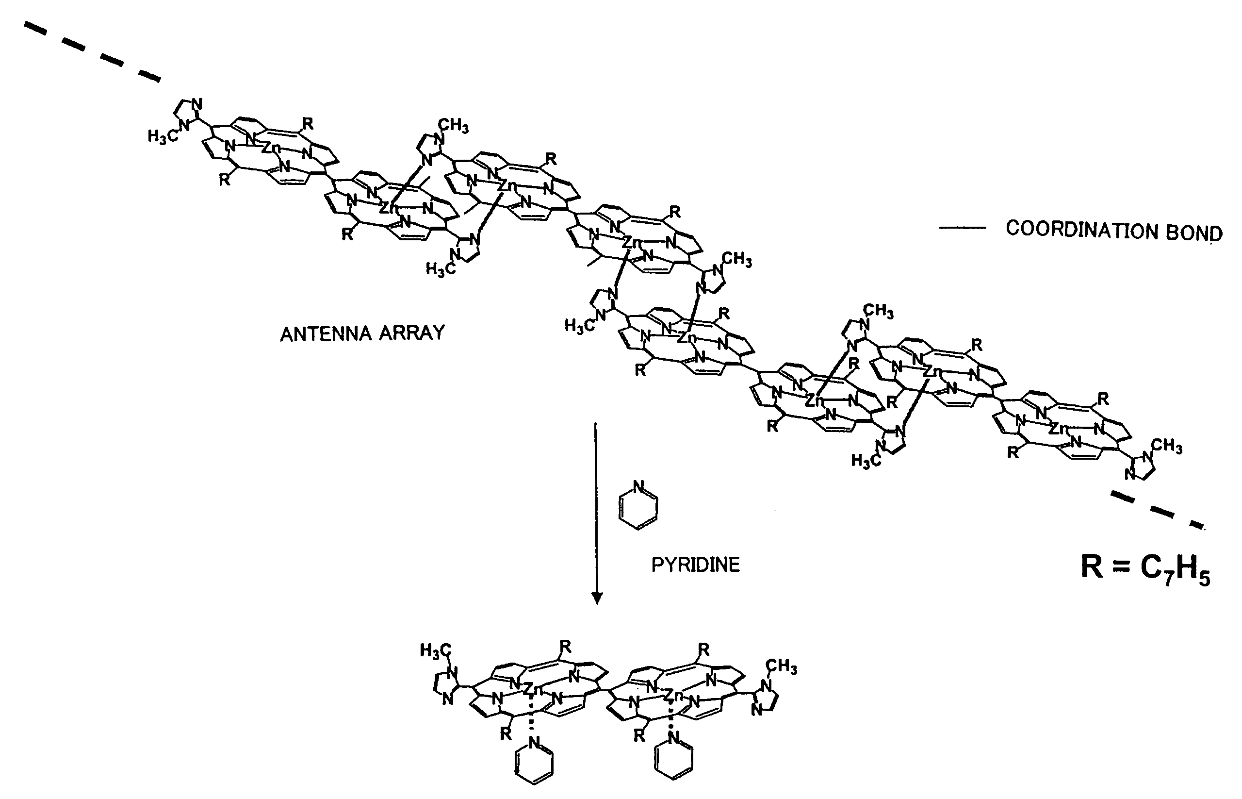
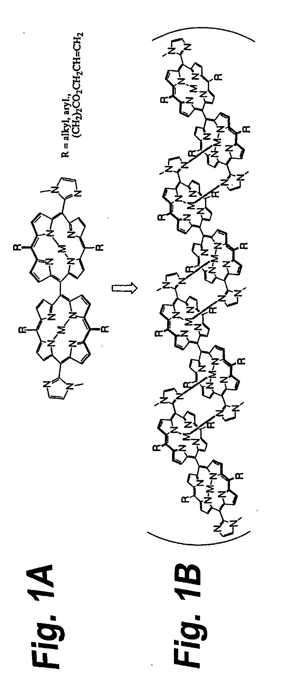
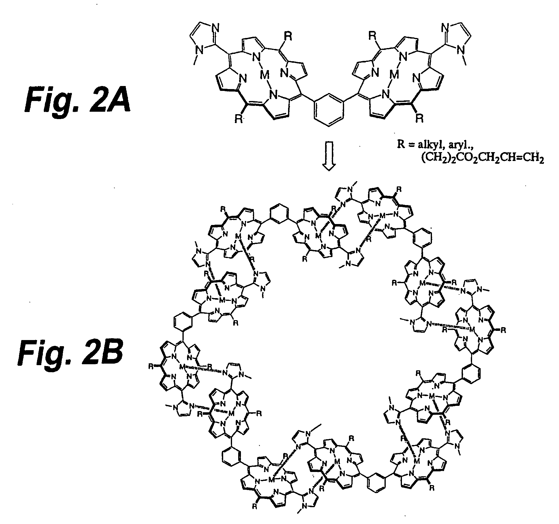
[0078] Further, a mixed solution of MEH-PPV, antenna porphyrin aggregate and PCBM (by the ratio of 1:1:4 in weight) (under chlorobenzene as the solvent) i...
PUM
| Property | Measurement | Unit |
|---|---|---|
| Electrical conductivity | aaaaa | aaaaa |
| Electrical resistance | aaaaa | aaaaa |
| Electrical conductor | aaaaa | aaaaa |
Abstract
Description
Claims
Application Information