Selective etch of films with high dielectric constant with H2 addition

a dielectric constant and selective etching technology, applied in the field of selective etching of films with high dielectric constant with h2 addition, can solve the problems of insufficient dielectric constant of ono to meet the ever increasing demand, and the difficulty of etching high k materials

Inactive Publication Date: 2007-03-15
LAM RES CORP
View PDF11 Cites 182 Cited by
  • Summary
  • Abstract
  • Description
  • Claims
  • Application Information

AI Technical Summary

Benefits of technology

[0008] To achieve the foregoing and in accordance with the purpose of the present invention, a method for selectively etching a high k layer with respect a silicon based material is provided. The high k layer over a silicon based layer is placed into an etch chamber. An etchant gas is provided into the etch chamber, wherein the etchant gas comprises H2. A plasma is generated from the etchant gas to selectively etch the high k layer with respect to the silicon based material.
[0009] In another manifestation of the invention, a method for etching a stack with a high k layer over a silicon based layer is provided. The stack is placed into an etch chamber. The high k layer is selectively etched with respect to the silicon based layer. The selective etching comprises providing a high k layer etchant gas into the etch chamber, wherein the high k layer etchant gas comprises H2 and generating a plasma from the high k layer etchant gas to selectively etch the high k layer with respect to the silicon based layer
[0010] In another manifestation of the invention, an apparatus for forming flash memory with a high k dielectric layer over a silicon based layer is provided. A plasma processing chamber, comprising a chamber wall forming a plasma processing chamber enclosure, a substrate support for supporting a substrate within the plasma processing chamber enclosure, a pressure regulator for regulating the pressure in the plasma processing chamber enclosure, at least one electrode for providing power to the plasma processing chamber enclosure for sustaining a plasma, a gas inlet for providing gas into the plasma processing chamber enclosure, and a gas outlet for exhausting gas from the plasma processing chamber enclosure is provided. A gas source is in fluid connection with the gas inlet and comprises an H2 gas source, a BCl3 gas source, and a Cl2 gas source. A controller is controllably connected to the gas source and the at least one electrode and comprises at least one processor and computer readable media. The computer readable media comprises computer readable code for selectively etching the high k layer with respect to the silicon based layer, computer readable code to stop the selectively etching the high k layer with respect to the silicon based layer, and computer readable code for selectively etching the silicon based layer with respect to the high k layer. The computer readable code for selectively etching the high k layer with respect to the silicon based layer comprises computer readable code for providing H2 from the H2 gas source, computer readable code for providing BCl3 from the BCl3 gas source, computer readable code for providing Cl2 from the Cl2 gas source, and computer readable code for generating a plasma from the H2, BCl3, and Cl2 to selectively etch the high k layer with respect to the silicon based layer.

Problems solved by technology

However, the dielectric constant of ONO is not enough to meet the ever increasing demand in operation voltage, so high dielectric constant material (or referred as to high k material) has been introduced to replace ONO.
Etching of high k material has been found to be more difficult compared to etching ONO, because of lower volatility of its etch byproduct.

Method used


Image

  • Selective etch of films with high dielectric constant with H2 addition
  • Selective etch of films with high dielectric constant with H2 addition
  • Selective etch of films with high dielectric constant with H2 addition

Examples


Embodiment Construction

[0020] The present invention will now be described in detail with reference to a few preferred embodiments thereof as illustrated in the accompanying drawings. In the following description, numerous specific details are set forth in order to provide a thorough understanding of the present invention. It will be apparent, however, to one skilled in the art, that the present invention may be practiced without some or all of these specific details. In other instances, well known process steps and / or structures have not been described in detail in order to not unnecessarily obscure the present invention.

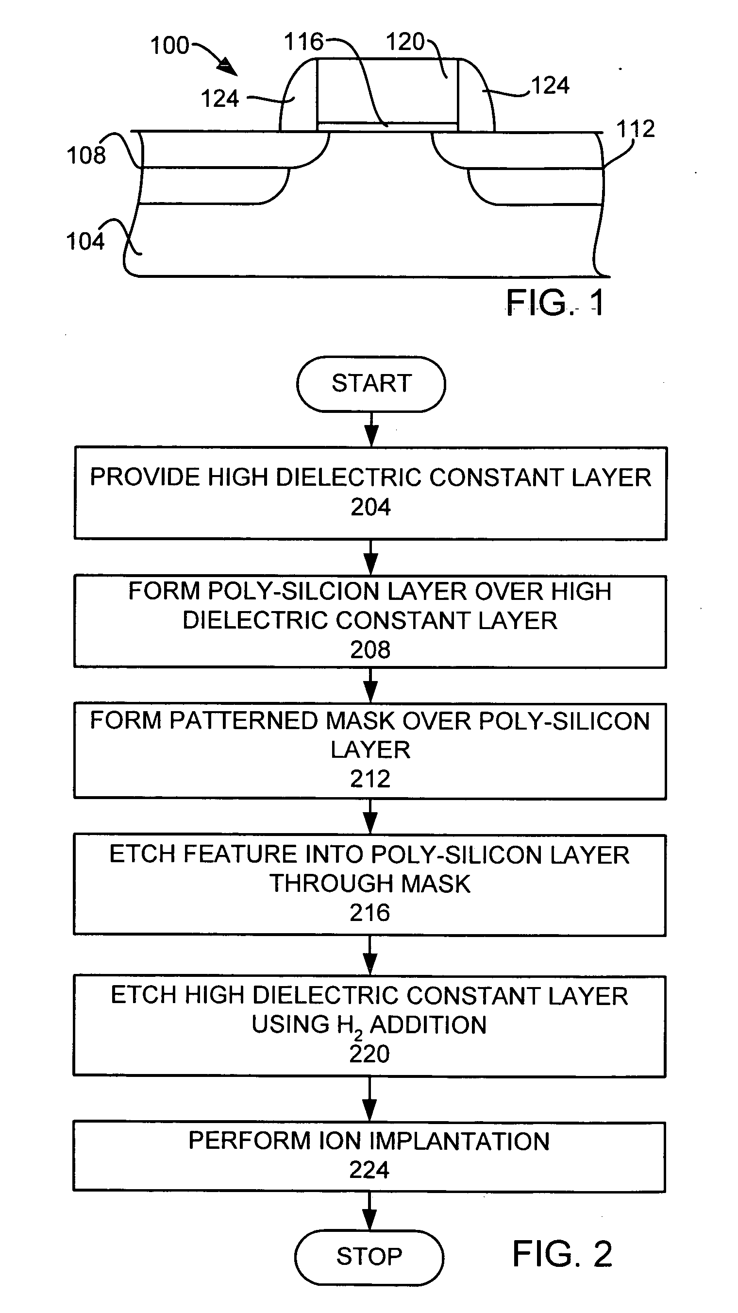
[0021] To facilitate understanding, FIG. 1 is a schematic view of a field effect transistor 100. The field effect transistor 100 comprises a substrate 104 into which a source 108 and a drain 112 are doped. A gate oxide 116 is formed over the substrate. A gate electrode 120 is formed over the gate oxide 116, so that the gate oxide 116 forms an insulator between the gate electrode 120 and ...


PUM

PropertyMeasurementUnit
dielectric constantaaaaaaaaaa

Abstract

A method for selectively etching a high k layer with respect to a silicon based material is provided. The high k layer is placed into an etch chamber. An etchant gas is provided into the etch chamber, wherein the etchant gas comprises H2. A plasma is generated from the etchant gas to selectively etch the high k layer with respect to a silicon based material.

Description

BACKGROUND OF THE INVENTION [0001] 1. Field of the Invention [0002] The invention relates to semiconductor devices. More specifically, the invention relates to semiconductor devices with a layer of a high dielectric constant material. [0003] 2. Description of the Related Art [0004] Since, flash memory is widely used in portable electronic devices, such as laptop computers, mobile phones, PDAs, etc, the demand to reduce operation voltage, so as to reduce energy consumption has been ever increasing. [0005] An ONO (oxide nitride oxide) layer has been used in flash memory device gate stack for memory storage. However, the dielectric constant of ONO is not enough to meet the ever increasing demand in operation voltage, so high dielectric constant material (or referred as to high k material) has been introduced to replace ONO. [0006] The dielectric constant of SiO2 is about 3.9. If high k material like Al2O3 is used to replace SiO2, the dielectric constant will increase to around 9.0. Oth...

Claims


Application Information

Patent Timeline
Patent Type & Authority Applications(United States)
IPC IPC(8): C23F1/00H01L21/306H01L21/302B44C1/22
CPCH01L21/31116H01L21/67069H01L21/31122H01L21/311
Inventor LIU, SHENJIANLEE, LINDA FUNG-MINGCHEN, ANTHONY
Owner LAM RES CORP
Why Eureka
Try Eureka